
Light-emitting device with sealing member comprising zinc sulfide particles

a technology of zinc sulfide particles and light-emitting devices, which is applied in the direction of semiconductor devices, basic electric elements, electrical appliances, etc., can solve the problems of deterioration of fluorescence efficiency, and easy deformation of semiconductor quantum dots surfaces, so as to achieve sufficient luminescence efficiency and stably emit light for a long time.

Active Publication Date: 2017-10-10
MATERIALS
View PDF29 Cites 0 Cited by
  • Summary
  • Abstract
  • Description
  • Claims
  • Application Information

AI Technical Summary

Benefits of technology

[0055]A light emitting device utilizing a semiconductor according to the present invention has sufficient luminescence efficiency, and is capable of stably emitting light for along time.

Problems solved by technology

Therefore, defects easily occur on surfaces of semiconductor quantum dots.
Defects on surfaces of semiconductor quantum dots act as various energy traps existing in a bandgap, and results in deterioration of the luminescence efficiency of the whole device.
In detail, dangling bonds (unsatisfied valences of atoms) on the surfaces and atomic vacancies cause an imbalance of electric charges, and excited electrons are trapped, so that fluorescence efficiency is deteriorated.
Due to the defects on the surfaces of the semiconductor quantum dots, the fluorescence efficiency deteriorates, and light from the light source becomes difficult to be wavelength-converted.
As a result, the luminescence efficiency of the whole device is deteriorated.
In addition, influences of various exogenous factors may cause defects on surfaces of semiconductor quantum dots.
However, at present, major causes are not clearly known.

Method used


Image

  • Light-emitting device with sealing member comprising zinc sulfide particles
  • Light-emitting device with sealing member comprising zinc sulfide particles
  • Light-emitting device with sealing member comprising zinc sulfide particles

Examples


first embodiment

[0089]In the present invention, by protecting the first sealing layer 50 including the semiconductor quantum dots 101 by the second sealing layer 60 with a moisture-proof property, a structure in which moisture such as environmental humidity hardly enters the first sealing layer 50 is obtained.

[0090]That is, even in a case where the LED light emitting device 5 is installed in an environment with high humidity, defects hardly occur on the surfaces of the semiconductor quantum dots. In addition, by the two-layer structure including the first sealing layer 50 and the second sealing layer 60, the semiconductor light emitting element can be protected from external factors such as heat and vibration. As a result, the LED light emitting device 5 can be made as a device having high luminescence efficiency and a long luminescence lifetime.

second embodiment

[0091]Subsequently, the present invention will be described.

[0092]FIG. 4 is a schematic view showing a structure of the second embodiment of the present invention.

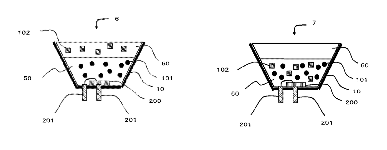
[0093]As shown in FIG. 4, the LED light emitting device 6 includes a package 10, a semiconductor light emitting element 200, a first sealing layer 50, and a second sealing layer 60. The first sealing layer 50 includes semiconductor quantum dots 101. Here, detailed description of members common with the first embodiment is omitted.

[0094]The LED light emitting device 6 includes zinc sulfide (ZnS) particles 102 in the second sealing layer 60. The ZnS particles 102 react with moisture derived from environmental humidity, etc., that enters the inside of the LED light emitting device 6 to reduce dissolution of ZnS of the shell portions of the semiconductor quantum dots 101 by moisture.

[0095]The ZnS particles 102 are blended so as to reach a concentration of approximately 0.5 percent by mass (wt %) in a mixed state with an epoxy ...

third embodiment

[0105]Subsequently, the present invention will be described.

[0106]FIG. 5 is a schematic view showing a structure of the third embodiment of the present invention.

[0107]As shown in FIG. 5, the LED light emitting device 7 includes a package 10, a semiconductor light emitting element 200, a first sealing layer 50, and a second sealing layer 60. In the first sealing layer 50, semiconductor quantum dots 101 are included. Here, detailed description of members common with the first embodiment and the second embodiment is omitted.

[0108]The LED light emitting device 7 includes ZnS particles 102 in the first sealing layer 50. The ZnS particles 102 react with moisture derived from environmental humidity, etc., entering the inside of the LED light emitting device 7, and reduce dissolution of ZnS of the shell portions of the semiconductor quantum dots 101 by moisture.

[0109]The ZnS particles 102 are blended so as to reach a concentration of approximately 0.5 percent by mass (wt %) in a mixed stat...


PUM


Abstract

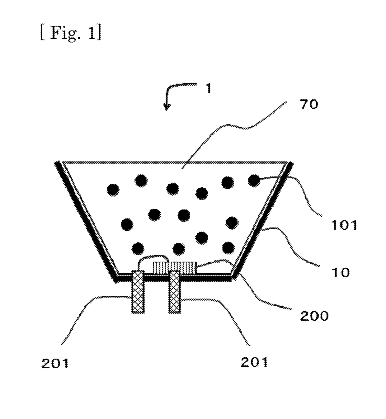
An LED light emitting device 5 as an example of a light emitting device utilizing a semiconductor to which the present invention is applied includes a package 10, a semiconductor light emitting element 200, a first sealing layer 50, and a second sealing layer 60. The semiconductor light emitting element 200 includes a p-n functioned semiconductor layer, and serves as a light source that emits light in accordance with application of a voltage to the semiconductor layer. The semiconductor light emitting element 200 is connected to power supply terminals 201 that supply a current.

Description

CROSS REFERENCE TO RELATED APPLICATIONS[0001]This patent application is a U.S. national stage application under 35 U.S.C. §371 of International Patent Application No. PCT / JP2013 / 068652 filed on Jul. 8, 2013. The International Application was published in Japanese on Jan. 15, 2015, as International Publication No. WO 2015 / 004711 A1 under PCT Article 21(2).TECHNICAL FIELD[0002]The present invention relates to a light emitting device utilizing a semiconductor. In detail, the present invention relates to a light emitting device utilizing a semiconductor which has sufficient luminescence efficiency and is capable of stably emitting light for a long time.BACKGROUND ART[0003]An LED element (light emitting diode) is a semiconductor element that emits light by application of a voltage, and is widely used due to high brightness, long life, and a characteristic of obtaining light not containing unnecessary ultraviolet rays or infrared rays. Asa use thereof, the LED element is applied to a ligh...

Claims


Application Information

Patent Timeline
Patent Type & Authority Patents(United States)
IPC IPC(8): H01L33/50H01L33/56H01L33/62
CPCH01L33/502H01L33/501H01L33/507H01L33/56H01L33/62H01L2224/48091H01L2924/181H01L2924/00012H01L2924/00014
Inventor KANAUMI, EIICHIKANENO, JUN
Owner MATERIALS
Learn More