Organic electroluminescent device and method for manufacturing same

a technology of electroluminescent devices and organic materials, applied in the direction of solid-state devices, discharge tubes/lamp details, natural mineral layered products, etc., can solve the problem of providing an organic light-emitting device with sufficient luminous efficiency, and achieve the effect of suppressing the influence of the first organic layer and high luminous efficiency

Active Publication Date: 2010-06-29
SANYO ELECTRIC CO LTD
View PDF10 Cites 0 Cited by
  • Summary
  • Abstract
  • Description
  • Claims
  • Application Information

AI Technical Summary

Benefits of technology

[0006]It is an object of the present invention to provide an organic electroluminescent device and a method of fabricating the same which provide sufficient luminous efficiency.

Problems solved by technology

The above-described prior art, however, has yet to provide an organic light emitting device with sufficient luminous efficiency.

Method used


Image

  • Organic electroluminescent device and method for manufacturing same
  • Organic electroluminescent device and method for manufacturing same
  • Organic electroluminescent device and method for manufacturing same

Examples


##ventive example 1

Inventive Example 1

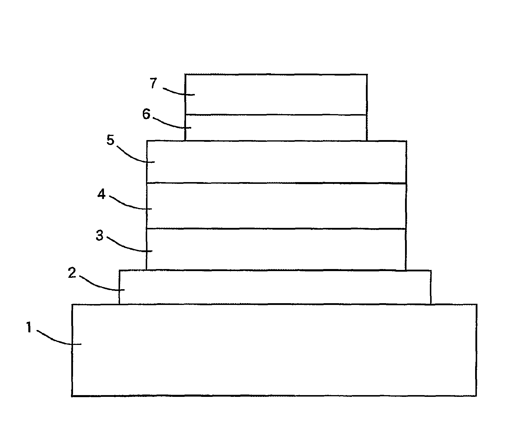
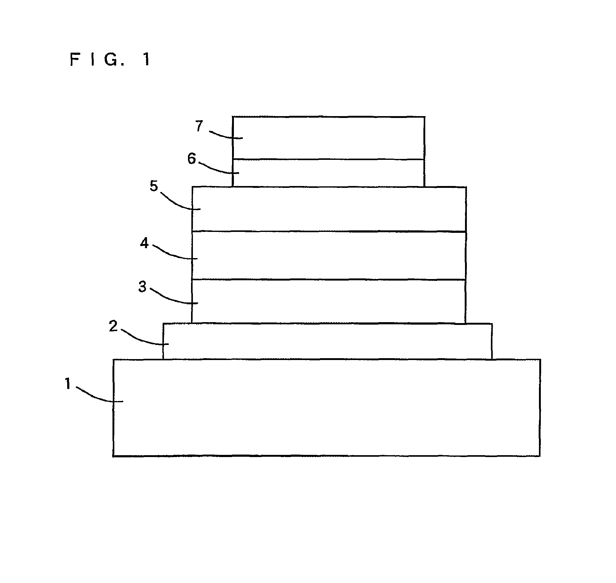
[0234]In Inventive Example 1, an organic electroluminescent device having a three-layered structure as shown in FIG. 1 was fabricated in a following method.

[0235]The method of fabricating the organic electroluminescent device according to the Inventive Example 1 will be described. A substrate 1 comprising an anode 2 made of ITO was used. Poly(ethylenedioxythiophene):poly(styrenesulphonate) (a mixture of poly(p-styrenesulfonic acid)salt of [2,3 -dihydrothieno(3,4,-b)(1,4)dioxin-5,7-diyl] and poly(p-styrenesulfonic acid)) (hereinafter called PEDOT:PSS) having a molecular structure represented by the formula (C1) below was formed to have a thickness of 40 nm on the anode 2 by spin coating, and baked at 180 degrees for ten minutes in the atmosphere, thus forming a hole injection layer 3.

[0236]

[0237]Then, MEH-PPV was formed to have a thickness of 40 nm on the hole injection layer 3 by spin coating, and baked at 80 degrees for five minutes in an atmosphere of nitrogen, ...

##ventive example 2

Inventive Example 2

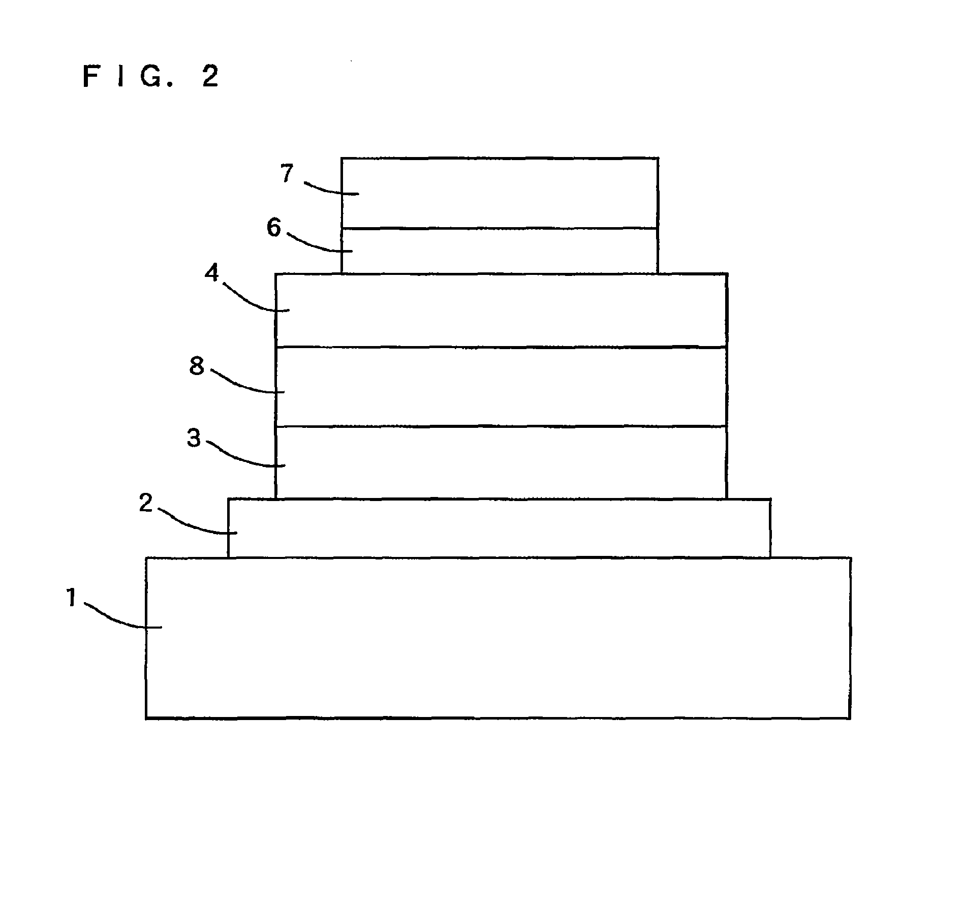
[0258]In Comparative Example 2, an organic electroluminescent device having the three-layered structure shown in FIG. 1 was fabricated in a following method.

[0259]Similarly in the Inventive Example 1, a glass substrate 1 comprising an anode 2 made of ITO was used. As with the Inventive Example 1, PEDOT:PSS was initially formed to have a thickness of 40 nm on the anode 2 by spin coating, and baked at 180 degrees for ten minutes in the atmosphere, thus forming a hole injection layer 3.

[0260]PF6-CVAP was subsequently formed to have a thickness of 40 nm on the hole injection layer 3 by spin coating, and baked at 80 degrees in an atmosphere of nitrogen, thus forming a light emitting layer 4. At this time, the PF6-CVAP was used as a solution of o-dichlorobenzene.

[0261]Then, PF8-DSB was formed to have a thickness of 40 nm on the light emitting layer 4 by spin coating, thus forming an electron transport layer 5 also serving as a hole blocking layer. At this time, the PF8-...

##ventive example 3

Inventive Example 3

[0272]In Inventive Example 3, nine kinds of organic electroluminescent devices having light emitting layers 4 and electron transport layers 5 in different thicknesses were fabricated to evaluate luminescent characteristics. The organic electroluminescent devices in the Inventive Example 3 are similar to the organic electroluminescent device in the Inventive Example 1 in structure and fabrication method except in the thicknesses of the light emitting layers 4 and the electron transport layers 5.

[0273]Table 4 shows thicknesses of the light emitting layer 4 and the electron transport layer 5 of each of the nine kinds of organic electroluminescent devices, 1-1, 1-2, 1-2, 2-1, 2-2, 2-3, 3-1, 3-2, 3-3.

[0274]

TABLE 4LIGHT EMITTINGLAYER THICKNESS (Å)INVENTIVE EXAMPLE 3140260620ELECTRON1601-12-13-1TRANSPORT LAYER3801-22-23-2THICKNESS (Å)6601-32-33-3

[0275](Evaluation 3)

[0276]The nine kinds of organic electroluminescent devices in the Inventive Example 3 were measured for lum...


PUM

PropertyMeasurementUnit
thicknessaaaaaaaaaa
thicknessaaaaaaaaaa
thicknessaaaaaaaaaa

Abstract

An organic electroluminescent device comprises a plurality of stacked layers of polymeric materials soluble in an organic solvent. As a polymeric material forming a lower layer, a polymeric material is selected having a molecular weight greater than the molecular weight of a polymeric material of a layer to be formed on the lower layer. As an organic solvent for dissolving the polymeric material forming the lower layer, an organic solvent is selected having a dielectric constant greater than the dielectric constant of an organic solvent for dissolving the polymeric material forming an upper layer. With a light emitting layer being the lower layer and an electron transport layer being the upper layer, it is preferable that the electron transport layer includes a polymeric material having hole blocking property. With a light emitting layer being the lower layer and an electron transport layer being the upper layer, it is preferable that the repeating unit of the polymeric material forming the light emitting layer and the repeating unit of the polymeric material forming the electron transport layer include the same chemical structure.

Description

TECHNICAL FIELD[0001]The present invention relates to an organic electroluminescent device and a method of fabricating the same.BACKGROUND ART[0002]Conventionally, in a low-molecular organic electroluminescent device, carriers are smoothly injected into a light emitting layer using a multi-layered structure formed with a dry process. In an organic electroluminescent device using polymeric materials, on the other hand, polymer layers are formed with a wet process. With the commonly used wet process, however, a polymer layer serving as a lower layer is subjected to dissolution during the formation of a polymer layer as an upper layer.[0003]For this reason, an organic electroluminescent device of the two-layered structure has been proposed in which two layers, a water-soluble conductive polymer and a luminescent polymer soluble in an organic solvent, are formed. Also proposed is the formation of a stacked structure using two kinds of solvents, a polar solvent and a non-polar solvent.[0...

Claims


Application Information

Patent Timeline
Patent Type & Authority Patents(United States)
IPC IPC(8): B05D5/06H01J1/62C08L65/00C09K11/06H01L51/00H01L51/30H01L51/50H01L51/56H05B33/00H05B33/10H05B33/12H05B33/14H05B33/22
CPCH01L51/50H01L51/0036Y10T428/24942H01L51/0038H01L51/0039H01L51/0042H01L51/0043H01L51/0052H01L51/0059H01L51/007H01L51/0081H01L51/5012H01L51/5048H01L51/56Y10S428/917H01L51/0037H10K85/1135H10K85/115H10K85/114H10K85/146H10K85/113H10K85/151H10K85/6565H10K85/615H10K85/631H10K85/324H10K50/14H10K50/00H10K50/11H10K71/00
Inventor HIRAYAMA, YASUKOSANO, TAKESHISAKAKIBARA, TAKAHISA
Owner SANYO ELECTRIC CO LTD
Why Eureka
Try Eureka