Differential circuit including a current mirror

a technology of mirrors and circuits, applied in the field of differential circuits, can solve the problems of increased mirror capacitance, decreased response speed, and increased number of elements, and achieve the effect of reducing response speed

Active Publication Date: 2018-04-24
ROHM CO LTD
View PDF10 Cites 0 Cited by
  • Summary
  • Abstract
  • Description
  • Claims
  • Application Information

AI Technical Summary

Benefits of technology

[0023]In view of the situation described above, it is a first object of the present invention to provide a differential circuit capable of suppressing the offset, a decrease of the response speed, and the number of elements.

Problems solved by technology

However, in this case, there is a problem that response speeds are decreased when the gains are increased so that mirror capacitances are increased.
However, there is a problem that the number of elements is increased.

Method used


Image

  • Differential circuit including a current mirror
  • Differential circuit including a current mirror
  • Differential circuit including a current mirror

Examples


first embodiment

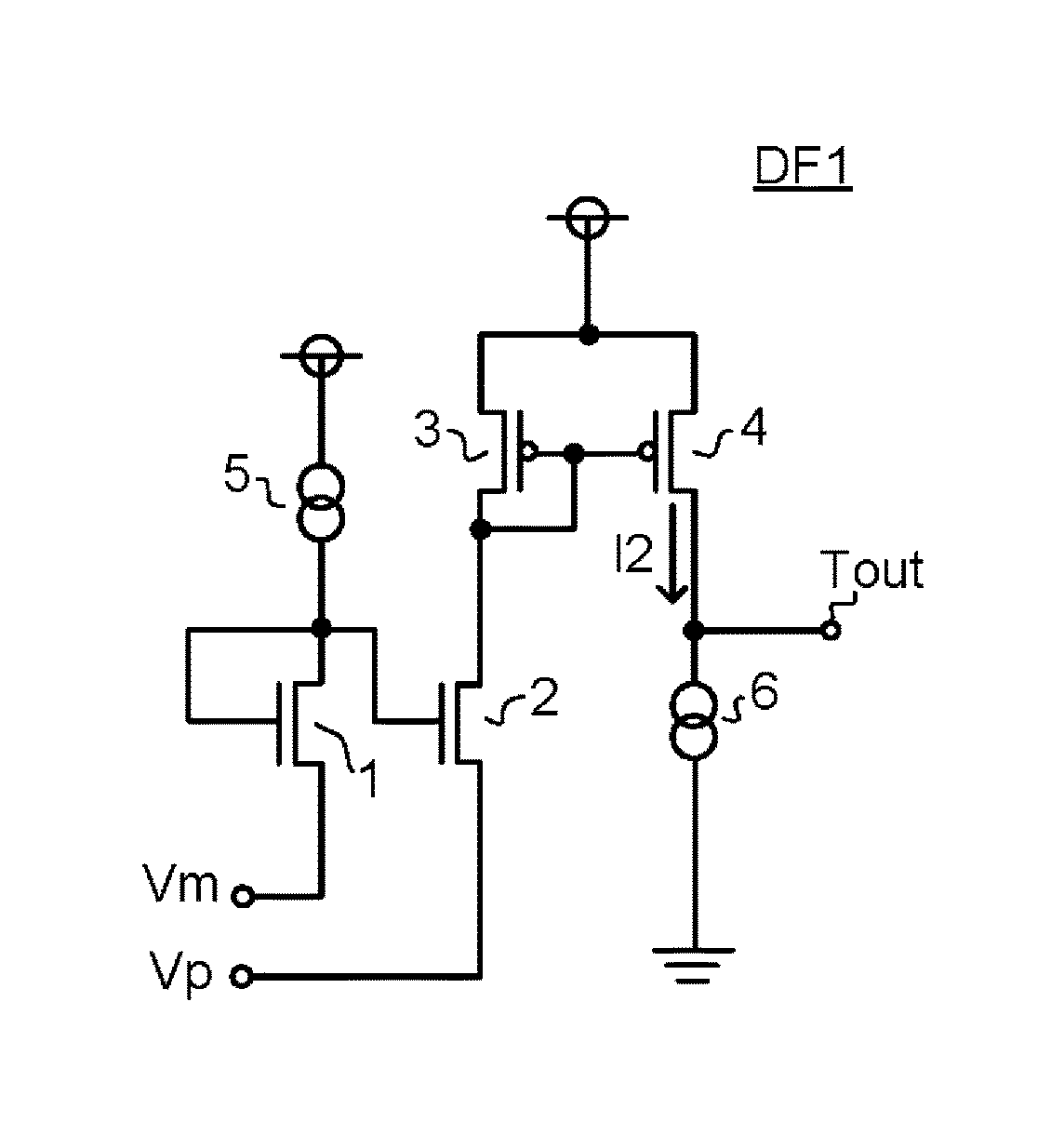
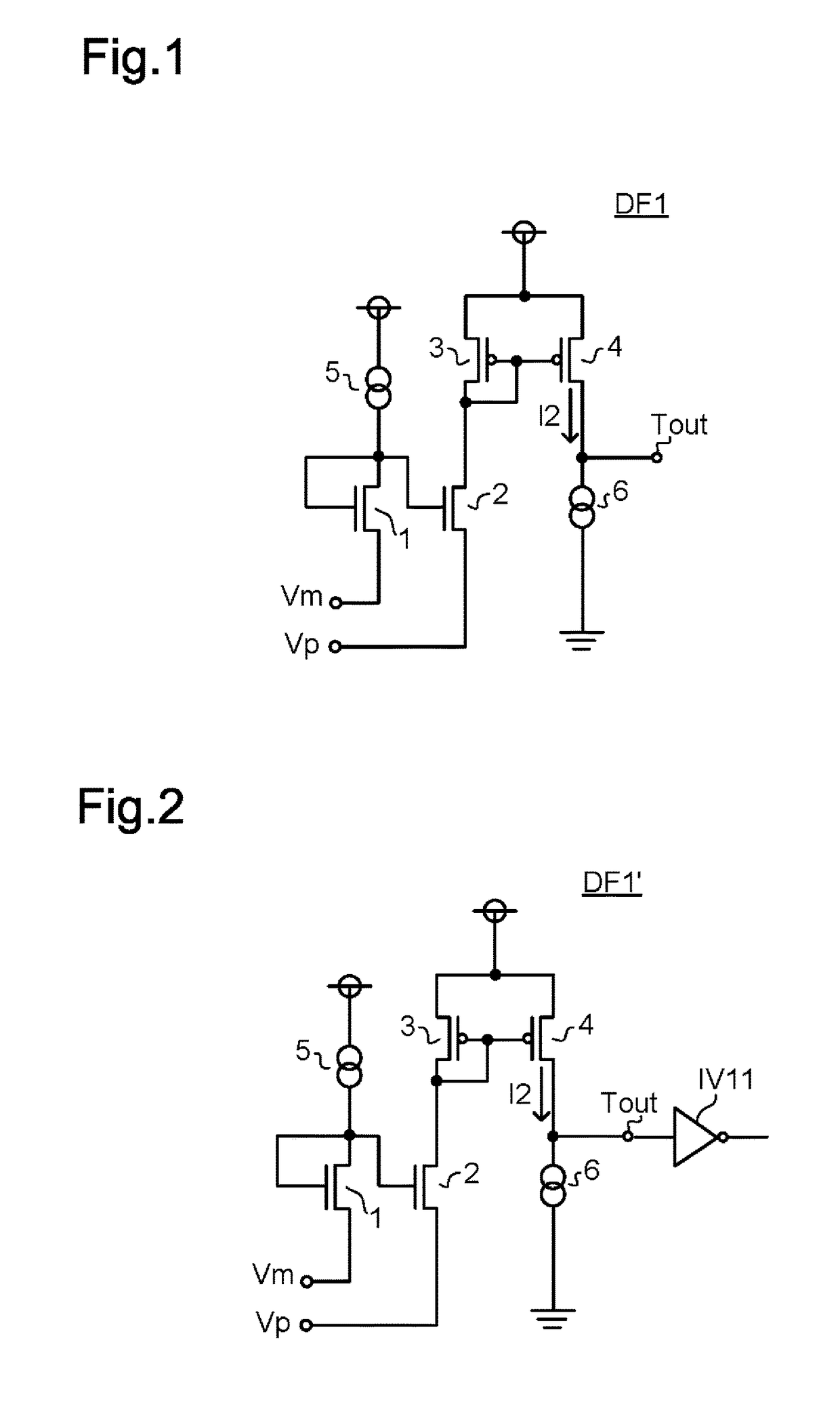
[0060]A circuit diagram of a differential circuit according to a first embodiment of the present invention is illustrated in FIG. 1.

[0061]A differential circuit DF1 illustrated in FIG. 1 includes transistors 1 to 4 and constant current circuits 5 and 6. The transistor 1 as an N-channel MOSFET having short-circuited drain and gate and the transistor 2 as an N-channel MOSFET constitute a first current mirror. The drain of the transistor 1 is connected to an application terminal of a power supply voltage via the constant current circuit 5. An input voltage Vm is applied to a source of the transistor 1.

[0062]An input voltage Vp is applied to a source of the transistor 2. The transistor 3 as a P-channel MOSFET having short-circuited drain and gate and the transistor 4 as a P-channel MOSFET constitute a second current mirror. The drain of the transistor 3 is connected to a drain of the transistor 2. Sources of the transistors 3 and 4 are connected to the application terminal of the power ...

second embodiment

[0098]FIG. 6 illustrates a circuit diagram of a differential circuit according to a second embodiment of the present invention. A differential circuit DF2 according to the second embodiment illustrated in FIG. 6 includes a differential main body portion D1 and an adjusting portion A1.

[0099]The differential main body portion D1 is constituted of transistors 21 to 28 and a constant current circuit 29. Sources of the transistors 21 and 22 as P-channel MOSFETs forming a differential pair are connected to an application terminal of the power supply voltage via the constant current source 29. The input voltage Vp is applied to a gate of the transistor 21, and an input voltage Vm is applied to a gate of the transistor 22.

[0100]The transistor 23 as an N-channel MOSFET having short-circuited drain and gate and the transistor 24 as an N-channel MOSFET constitute a first current mirror, and the drain of the transistor 23 is connected to a drain of the transistor 21. Sources of the transistors ...

third embodiment

[0113]Next, a third embodiment of the present invention is described. A circuit diagram of a differential circuit of this embodiment is illustrated in FIG. 8.

[0114]A differential circuit DF3 according to the third embodiment illustrated in FIG. 8 includes a differential main body portion D2 and an adjusting portion A2. The differential main body portion D2 includes transistors 41 to 48 and a constant current circuit 49, having the same structure as the differential main body portion D1 in the second embodiment, and hence detailed description thereof is omitted.

[0115]In addition, the adjusting portion A2 includes a transistor 51 as a P-channel MOSFET having a gate to which an input voltage V51 is applied, a transistor 52 as a P-channel MOSFET having a gate to which an input voltage V52 is applied, and a constant current circuit 53. Sources of the transistors 51 and 52 are connected to the application terminal of the power supply voltage via the constant current circuit 53. A drain of...


PUM


Abstract

A differential circuit includes a first constant current circuit, a second constant current circuit having the same constant current value as the first constant current circuit, a current mirror including a first transistor having a current sink terminal connected to the first constant current circuit, a current drain terminal to which a first input voltage is applied, and a gate short-circuited to the current sink terminal, and a second transistor having a gate connected to the current sink terminal of the first transistor and a current drain terminal to which a second input voltage is applied, and a current output terminal connected to a connection node between a part in which a current based on an output current of the current mirror flows and the second constant current circuit.

Description

CROSS-REFERENCE TO RELATED APPLICATIONS[0001]This nonprovisional application claims priority under 35 U.S.C. § 119(a) on Patent Applications No. 2015-024282 and No. 2015-024291 filed in Japan on Feb. 10, 2015, the entire contents of which are hereby incorporated by reference.BACKGROUND OF THE INVENTION[0002]Field of the Invention[0003]The present invention relates to a differential circuit.[0004]Description of Related Art[0005]Conventionally, there is known a differential circuit, which outputs a current corresponding to a difference between two input voltages. FIG. 14 illustrates an example of a conventional differential circuit.[0006]A conventional differential circuit DF100 illustrated in FIG. 14 includes transistors 101 to 108 and a constant current circuit 109. Sources of the transistors 101 and 102, which are P-channel MOS field effect transistors (MOSFETs) forming a differential pair, are connected to an application terminal of a power supply voltage via the constant current ...

Claims


Application Information

Patent Timeline
Patent Type & Authority Patents(United States)
IPC IPC(8): G05F3/26H02M1/32H02M1/00
CPCG05F3/262H02M1/32H02M2001/0009H02M1/0009
Inventor AKAHO, TADASHI
Owner ROHM CO LTD
Why Eureka
Try Eureka