Method for producings uper-resolution micro structure diffraction optical element
A technique for diffractive elements and manufacturing methods, applied to optical elements, diffraction gratings, optics, etc., can solve problems such as difficulty in realization, contamination of recording media, and difficulty in operation, and achieve simple and easy process, low surface roughness, and safety Good results
- Summary
- Abstract
- Description
- Claims
- Application Information
AI Technical Summary
Problems solved by technology
Method used
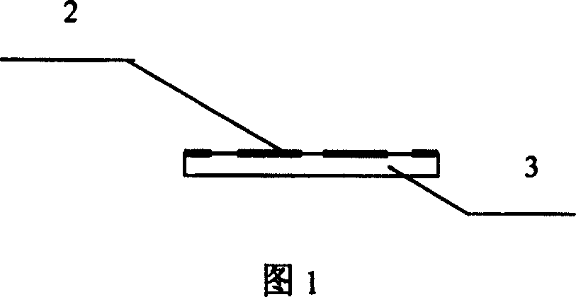
Image

Examples
Embodiment 1
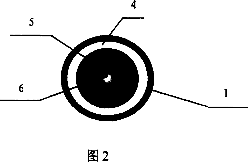
[0018] With reference to Fig. 1, 2, a kind of fabrication method of super-resolution microstructure diffraction element comprises the following steps: (1) prepare the photolithography mask plate with super-resolution diffraction figure with conventional ultraviolet lithography mask plate making technology, described photolithography The engraving mask is a chrome plate, and the working area of the mask is a circle, and the circle is closely surrounded by a central circle, an intermediate ring and a peripheral ring in sequence, the outer diameter of the peripheral ring is 1.0 cm, and the inner diameter of the intermediate ring is 1.0 cm. and outer diameters of 0.04 cm and 0.95 cm; (2) Coating a layer of 103-B UV negative photoresist on the UV-transmitting quartz glass through routine cleaning, and curing with a hot plate, the baking temperature is 75 DEG C, and the baking time is 20 minutes; (3) carry out photoetching to photoresist with ultraviolet lithography method, the pho...
Embodiment 2
[0020] A method for making a super-resolution microstructure diffraction element, comprising the following steps: (1) preparing a photolithography mask with a super-resolution diffraction pattern using a conventional ultraviolet lithography mask manufacturing technique, the photolithography mask being a chrome plate , the working area of the reticle is a circle, and the circle is closely surrounded by a central circle, an intermediate ring and a peripheral ring in sequence, the outer diameter of the peripheral ring is 1.0 cm, and the inner and outer diameters of the middle ring are 0.04 cm and 0.95 cm; (2) Coating a layer of 103-B UV negative photoresist on the UV-transparent quartz glass through conventional cleaning treatment, and baking and curing with a hot plate, the baking temperature is 85 ° C, and the baking temperature is 85 ° C. The time is 15 minutes; (3) carry out photoetching to photoresist with ultraviolet lithography method, the photoetching mask plate that ado...
Embodiment 3
[0022] A method for making a super-resolution microstructure diffraction element, comprising the following steps: (1) preparing a photolithography mask with a super-resolution diffraction pattern using a conventional ultraviolet lithography mask manufacturing technique, the photolithography mask being a chrome plate , the working area of the reticle is a circle, and the circle is tightly surrounded by a central circle, an intermediate ring and a peripheral ring in sequence, the outer diameter of the peripheral ring is 1.0 cm, and the inner and outer diameters of the intermediate ring are 0.04 cm and 0.95 cm; (2) Coat a layer of 103-B UV negative photoresist on the UV-transmitting quartz glass that has been conventionally cleaned, and bake and cure with a hot plate, and the baking temperature is 80°C. Baking time It was 18 minutes; (3) carry out photoetching to photoresist with ultraviolet lithography method, the photoetching mask plate that adopts is the chrome plate that ste...
PUM
 Abstract
Description
Claims
Application Information
 - R&D
- Intellectual Property
- Life Sciences
- Materials
- Tech Scout
- Unparalleled Data Quality
- Higher Quality Content
- 60% Fewer Hallucinations
Browse by: Latest US Patents, China's latest patents, Technical Efficacy Thesaurus, Application Domain, Technology Topic, Popular Technical Reports.
© 2025 PatSnap. All rights reserved.Legal|Privacy policy|Modern Slavery Act Transparency Statement|Sitemap|About US| Contact US: help@patsnap.com