Display array and display panel

A technology for display panels and display units, applied in the field of display arrays, capable of solving problems such as differences in brightness, uneven display, and differences in threshold voltage values ​​of driving transistors

Active Publication Date: 2008-07-30
AU OPTRONICS CORP
View PDF7 Cites 0 Cited by
  • Summary
  • Abstract
  • Description
  • Claims
  • Application Information

AI Technical Summary

Problems solved by technology

[0007] However, due to the manufacturing process of thin film transistors, in the display array 12, the electrical characteristics of the driving transistors in each region are different, that is, the threshold voltage values ​​of the driving transistors are different.
Therefore, when a plurality of display units in different regions receive video signals with the same voltage, due to differences in the threshold voltages of the driving transistors, the value of the driving current supplied to the organic light-emitting diodes in these display units is inconsistent, resulting in organic The brightness emitted by the light-emitting diodes is different, and panel 1 displays an uneven picture

Method used


Image

  • Display array and display panel
  • Display array and display panel
  • Display array and display panel

Examples


Embodiment Construction

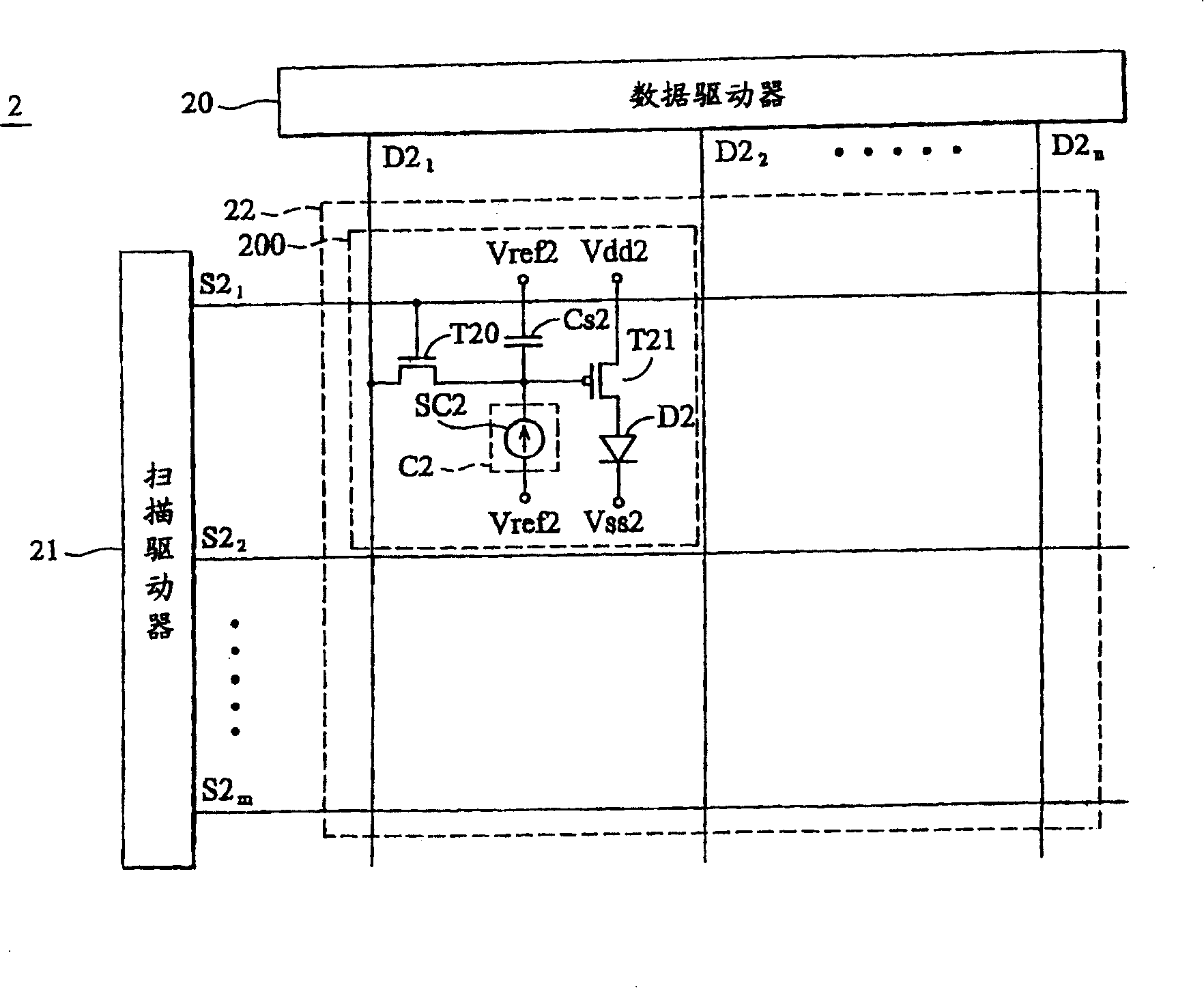
[0017] figure 2 It is a schematic diagram showing the panel of the organic light emitting display device of the present invention. The panel 2 includes a data driver 20 , a scan driver 21 and a display array 22 . Data driver 20 controls multiple data lines D2 1 to D2 n , and the scan driver 21 controls a plurality of scan lines S2 1 to S2 m . Data line D2 1 to D2 n and scan line S2 1 to S2 m It is provided on a substrate (not shown) of the panel 2 . The display array 22 is composed of data lines D2 interleaved in pairs 1 to D2 n and scan line S2 1 to S2 m Formed, and each staggered data line and scan line form a display unit, for example, data line D2 1 and scan line S2 1 The display unit 200 is formed. As shown in the figure, the equivalent circuit of the display unit 200 (other display units are the same) includes a switching transistor T20, a storage capacitor Cs2, a driving transistor T21, an OLED D2 and a control unit C2.

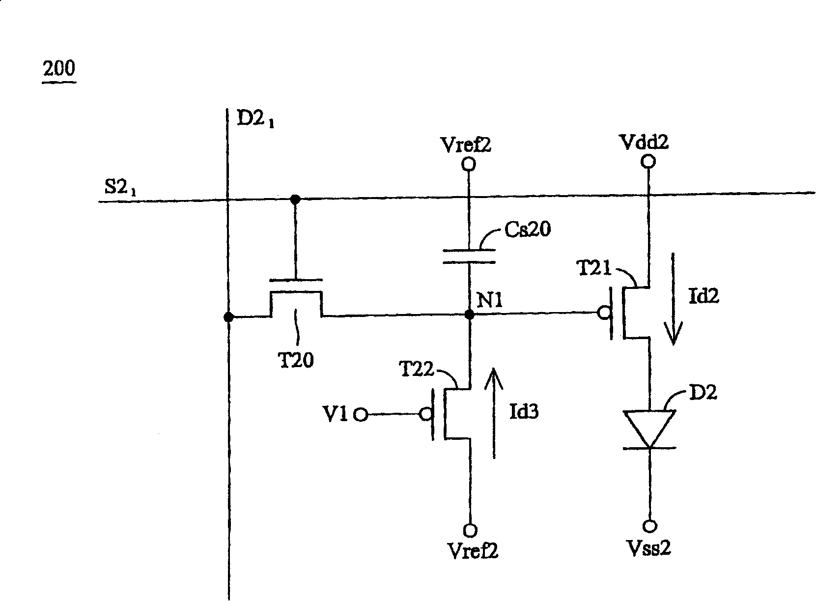
[0018] Such as image 3 As sh...


PUM


Abstract

The display array is suitable to faceplate of organic luminous display device. The display array includes multiple data lines, multiple scan lines and multiple display units. Each display unit is corresponding to a group of scanning lines and data lines, and each display unit includes control unit, driving transistor and light-emitting diode (LED). Based on drive capability of driving transistor, control unit in each display unit adjusts magnitude of luminous intensity of LED in the display unit at fixed luminous time.

Description

technical field [0001] The present invention relates to a display array, in particular to a display array suitable for an organic light-emitting display device. Background technique [0002] figure 1 It is a schematic diagram showing a panel of a known organic light emitting display device. The panel 1 includes a data driver 10 , a scan driver 11 and a display array 12 . Data driver 10 controls multiple data lines D1 1 to D1 n , and the scan driver 11 controls a plurality of scan lines S1 1 to S1 m . The display array 12 is composed of data lines D1 interleaved in pairs 1 to D1 n and scan line S1 1 to S1 m Formed, and each staggered data line and scan line form a display unit, for example, data line D1 1 and scan line S1 1 The display unit 100 is formed. As shown in the figure, the equivalent circuit of the display unit 100 (other display units are the same) includes a switching transistor T10, a storage capacitor Cs1, a driving transistor T11, and an organic li...

Claims


Application Information

Patent Timeline
Patent Type & Authority Patents(China)
IPC IPC(8): G09G3/32G09G3/30G09G3/3266G09G3/3283G09G3/3291
Inventor 施立伟李纯怀
Owner AU OPTRONICS CORP
Why Eureka
Try Eureka