Compensation system and method for oled display panel

A display panel and compensation system technology, applied in the field of compensation system of OLED display panels, can solve the problems of different luminous efficiency, increased cost, and reduced display quality of OLED display devices, etc., to reduce storage space, improve picture uniformity, and compensate for display The effect of unevenness

Active Publication Date: 2020-09-29
WUHAN CHINA STAR OPTOELECTRONICS SEMICON DISPLAY TECH CO LTD
View PDF6 Cites 0 Cited by
  • Summary
  • Abstract
  • Description
  • Claims
  • Application Information

AI Technical Summary

Problems solved by technology

Usually AMOLED pixel driving circuits are equipped with driving thin film transistors for driving organic light emitting diodes to emit light. During use, due to the aging of organic light emitting diodes and the shift of the threshold voltage of driving thin film transistors, the display of OLED display devices The quality is degraded, so it is necessary to detect and compensate the threshold voltage of the driving thin film transistor during the use of the OLED display device, so as to ensure the display quality of the OLED display device
[0005] Although some compensation techniques solve the influence of Vth, the cost is that the complex compensation circuit reduces the pixel aperture ratio, and there is also a certain limit on the number of pixels per inch of the display panel. The evaporation process leads to characteristic differences between sub-pixels, such as OLED The cross-voltage and luminous efficiency are different. The existing solution is to use external optical compensation to make the panel display normally, but the external optical compensation needs to use expensive memory, and as the screen size increases, the memory space doubles. , thus greatly increasing the cost; and still unable to solve the impact of OLED device aging

Method used


Image

  • Compensation system and method for oled display panel
  • Compensation system and method for oled display panel
  • Compensation system and method for oled display panel

Examples


Embodiment Construction

[0048] In order to further illustrate the technical means adopted by the present invention and its effects, the following describes in detail in conjunction with preferred embodiments of the present invention and accompanying drawings.

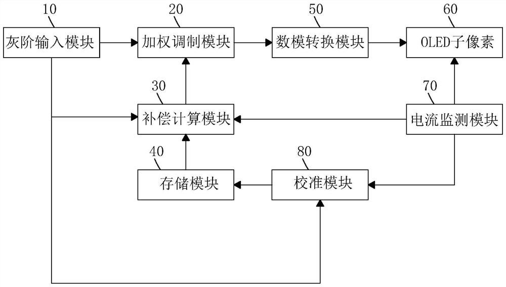
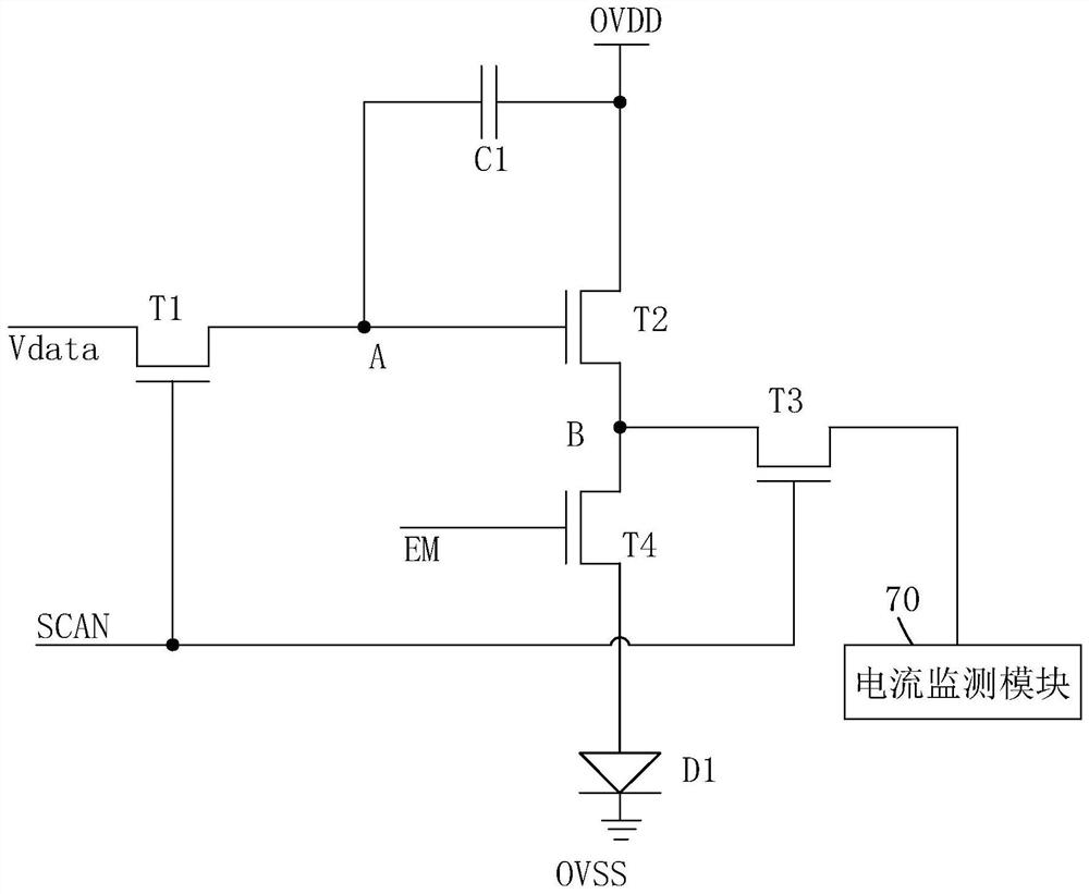
[0049] see figure 1 , the present invention provides a compensation system for an OLED display panel, comprising: a grayscale input module 10, a weighted modulation module 20 connected to the grayscale input module 10, and both the grayscale input module 10 and the weighted modulation module 20 The connected compensation calculation module 30, the digital-to-analog conversion module 50 connected to the weighted modulation module 20, the OLED sub-pixel 60 connected to the digital-to-analog conversion module 50, and the OLED sub-pixel 60 and the compensation calculation module 30 are all connected current monitoring module 70;

[0050] The gray scale input module 10 is configured to provide an initial gray scale to the weighted modulation modul...


PUM


Abstract

A compensation system and method for an organic light-emitting diode (OLED) display panel. The compensation system comprises: a gray scale input module (10), a weighting modulation module (20), a compensation calculation module (30), a digital-to-analogue conversion module (50), OLED sub-pixels (60) and a current monitoring module (70). The compensation calculation module (30) may calculate a target feedback current corresponding to an initial gray scale according to an initial gray scale inputted by the gray scale input module (10), a pre-measured modulation coefficient and maximum feedback current and calculate a weighting coefficient according to the target feedback current and an actual feedback current of the OLED sub-pixels (60) monitored by the current monitoring module (70); the weighting modulation module (20) may adjust the initial gray scale according to the weighting coefficient to obtain a target gray scale and utilize the target gray scale to illuminate the OLED sub-pixels (60), so that the phenomenon of nonuniform display caused by ageing of an organic light emitting diode may be compensated for, the storage space required by a compensation system is decreased, and the picture uniformity of the display panel is improved.

Description

technical field [0001] The invention relates to the field of display technology, in particular to a compensation system and method for an OLED display panel. Background technique [0002] Organic light emitting diode (Organic Light Emitting Display, OLED) display device has self-illumination, low driving voltage, high luminous efficiency, short response time, high definition and contrast, nearly 180° viewing angle, wide operating temperature range, and can realize flexible display and With many advantages such as large-area full-color display, it is recognized by the industry as a display device with the most potential for development. [0003] OLED display devices can be divided into passive matrix OLED (Passive Matrix OLED, PMOLED) and active matrix OLED (Active Matrix OLED, AMOLED) two categories according to the driving method, namely direct addressing and thin film transistor (Thin Film Transistor, TFT) matrix addressing two types. Among them, AMOLED has pixels arrang...

Claims


Application Information

Patent Timeline
Patent Type & Authority Patents(China)
IPC IPC(8): G09G3/3208
CPCG09G3/3208
Inventor 颜伟男
Owner WUHAN CHINA STAR OPTOELECTRONICS SEMICON DISPLAY TECH CO LTD
Why Eureka
Try Eureka