Array structure of transverse electric field effect type and its manufacturing method

A liquid crystal display, lateral electric field technology, applied in semiconductor/solid-state device manufacturing, static indicators, instruments, etc., can solve problems such as electric field confusion between electrodes, and achieve the effects of preventing poor contact, suppressing flickering, and improving aperture ratio

Active Publication Date: 2008-09-03
INNOLUX CORP
View PDF4 Cites 3 Cited by
  • Summary
  • Abstract
  • Description
  • Claims
  • Application Information

AI Technical Summary

Problems solved by technology

That is, due to the electric field leaked from the gate line 112, the electric field between the electrodes is disturbed

Method used


Image

  • Array structure of transverse electric field effect type and its manufacturing method
  • Array structure of transverse electric field effect type and its manufacturing method
  • Array structure of transverse electric field effect type and its manufacturing method

Examples


Embodiment Construction

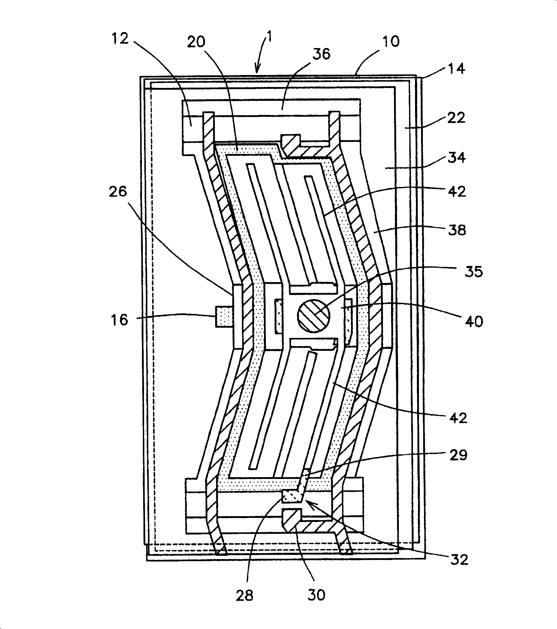
[0080] The IPS liquid crystal display of the first embodiment of the present invention is manufactured by the following steps (1) to (8) in the same manner as the above-mentioned prior art IPS liquid crystal display 101 . That is, refer to Figure 18 , (1) Prepare a transparent insulating substrate such as an insulating substrate. (2) Form the gate line 62, the hollow wing portion 70, and the capacitive electrode 66 having an electrode portion on a glass substrate. (3) The first insulating layer 64 is formed by the CVD method. (4) Form on the insulating layer 64: the signal line 74, connected to the TFT 82 with a part of the gate line 62 as the gate electrode, the drain electrode 80 of the TFT 82; the counter electrode 76, via the first insulating layer 64 facing the electrode portion of the capacitance electrode; and an intra-pixel wiring 79 for connecting the counter electrode 76 and the source electrode 78 of the TFT 82 . (5) The second insulating layer 72 is formed on t...


PUM


Abstract

The invention provides an IPS liquid crystal display with a Cs line disposed in the vicinity of a gate line in which a flicker and image persistence of a liquid crystal display is suppressed by shielding influence of an electric field diverging from the gate line. In the IPS liquid crystal display, a pixel surrounded by a first common electrode line includes the gate lines laid on an insulating substrate in parallel to each other, a first insulating film covering the gate lines and a Cs line with a wing part laid on the first insulating film in parallel to the gate lines between the neighboring gate lines wherein the hollow wing part of the Cs line is laid in the proximity of the gate lines at the end parts.

Description

technical field [0001] The present invention relates to a liquid crystal display, in particular to an IPS liquid crystal display which can shield the influence of an electric field from a grid line without lowering the aperture ratio, and is less likely to cause display burns. Background technique [0002] The IPS (In-Plane Switching) method used to obtain liquid crystals with a wide viewing angle makes the applied electric field parallel to the substrate surface, also known as the lateral electric field effect method. In the IPS method, the arrangement of liquid crystal molecules in the substrate plane is changed by turning ON / OFF of an electric field along the substrate. In addition, this characteristic change in molecular arrangement produces an epoch-making wide viewing angle that cannot be seen in longitudinal electric field effect methods such as the twisted nematic (Twisted Nematic; TN) method. Hereinafter, an IPS liquid crystal display is referred to as an IPS liqui...

Claims


Application Information

Patent Timeline
Patent Type & Authority Patents(China)
IPC IPC(8): G02F1/1343G02F1/1368G02F1/133G02F1/136H01L21/00H01L29/786
Inventor 广升泰信草深薰池崎充
Owner INNOLUX CORP
Why Eureka
Try Eureka