
Chip testing method and related devices

A chip testing and chip technology, which is applied in the field of chip testing and related devices, can solve the problem of inability to judge the position of the trigger edge of the data indication signal, the inability to know whether the timing relationship between the data indication signal and the data signal is correct, and the inability to show the performance of chip output and output and other issues to achieve the effect of reducing the overall cost

Active Publication Date: 2009-03-11
VIA TECH INC
View PDF6 Cites 0 Cited by
  • Summary
  • Abstract
  • Description
  • Claims
  • Application Information

AI Technical Summary

Problems solved by technology

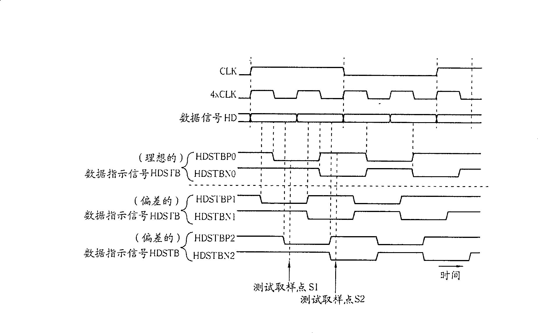
However, in the traditional technology, because the tester can only sample the data indication signal at a specific time point, it cannot judge the trigger edge position of the data indication signal, so it is impossible to know whether the timing relationship between the data indication signal and the data signal is correct
In other words, the test results of traditional technology cannot completely and truly show the input and output performance of the chip

Method used


Image

  • Chip testing method and related devices
  • Chip testing method and related devices
  • Chip testing method and related devices

Examples


Embodiment Construction

[0020] Hereinafter, embodiments of the present invention will be described in detail with reference to the drawings.

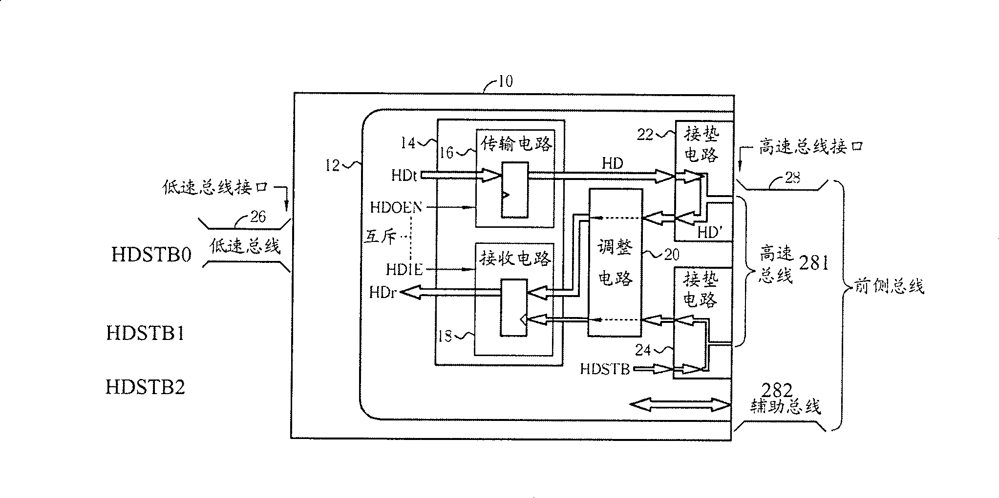
[0021] Please refer to figure 1 ; figure 1 It is a functional block diagram of a chip 10, and the chip 10 can be a chipset. One end of the chip 10 is connected to a front-side bus 28 , and the other end is connected to at least one low-speed bus 26 . The chip 10 can be connected to a central processing unit (CPU) via the front side bus 28 figure 1 not shown in). And through the low-speed bus 26, the chipset 10 can be connected with other peripheral electronic circuits / chips / electronic devices, such as memory, video capture devices (such as video cameras) and even various non-volatile storage devices (such as hard disks). computer, optical drive, etc.).

[0022] The front side bus 28 has a bidirectional high-speed bus 281 and an auxiliary bus 282 . The auxiliary bus 282 is used to transmit information such as instructions and addresses, while the high-spe...


PUM


Abstract

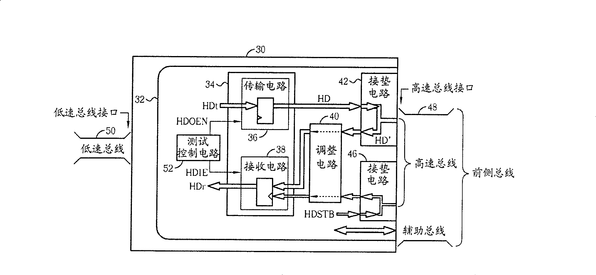
The related chip testing method comprises: to test dual-direction high-speed bus, transmitting the testing signal into chip through low-speed bus, letting the high-speed bus transmission mechanism to send the testing signal to the high-speed bus interface, and also letting the receiving mechanism form an inner loop and back transmit the information by low-speed bus. Thereby, this invention can save testing cost.

Description

technical field [0001] The invention relates to a chip testing method and a related device, in particular to a chip testing method and a related device with a high-speed bus interface tested in a low-speed testing environment. Background technique [0002] In an electronic system, different electronic circuits / chips exchange information with each other through a bus, so that the electronic circuits / chips can coordinate their operations and integrate their respective functions to achieve the overall function of the electronic system. For example, in a computer system, the central processing unit is bridged to other peripheral devices (such as hard drives, optical drives, display cards, etc.) They will be connected to each other by a bus, so that the above-mentioned electronic circuits / chips can be integrated and operated. Of course, in the modern information society that emphasizes efficiency, the performance requirements for electronic systems are also increasing. In order...

Claims


Application Information

Patent Timeline
Patent Type & Authority Patents(China)
IPC IPC(8): G01R31/28G01R31/317G01R31/3185G06F11/267
Inventor 徐祥哲谢博伟
Owner VIA TECH INC
Learn More