Thin film transistor module base board and its making method

A technology of a thin film transistor and a manufacturing method, applied in the field of liquid crystal display components, can solve problems such as environmental pollution, and achieve the effects of improving quality and increasing stability

Inactive Publication Date: 2009-08-05
CHUNGHWA PICTURE TUBES LTD
View PDF3 Cites 0 Cited by
  • Summary
  • Abstract
  • Description
  • Claims
  • Application Information

AI Technical Summary

Problems solved by technology

[0006] The object of the present invention is to provide a thin film transistor array substrate, which has a light-shielding structure in the non-display area, and this light-shielding structure can improve the problem of environmental pollution in the prior art

Method used


Image

  • Thin film transistor module base board and its making method
  • Thin film transistor module base board and its making method
  • Thin film transistor module base board and its making method

Examples


Embodiment Construction

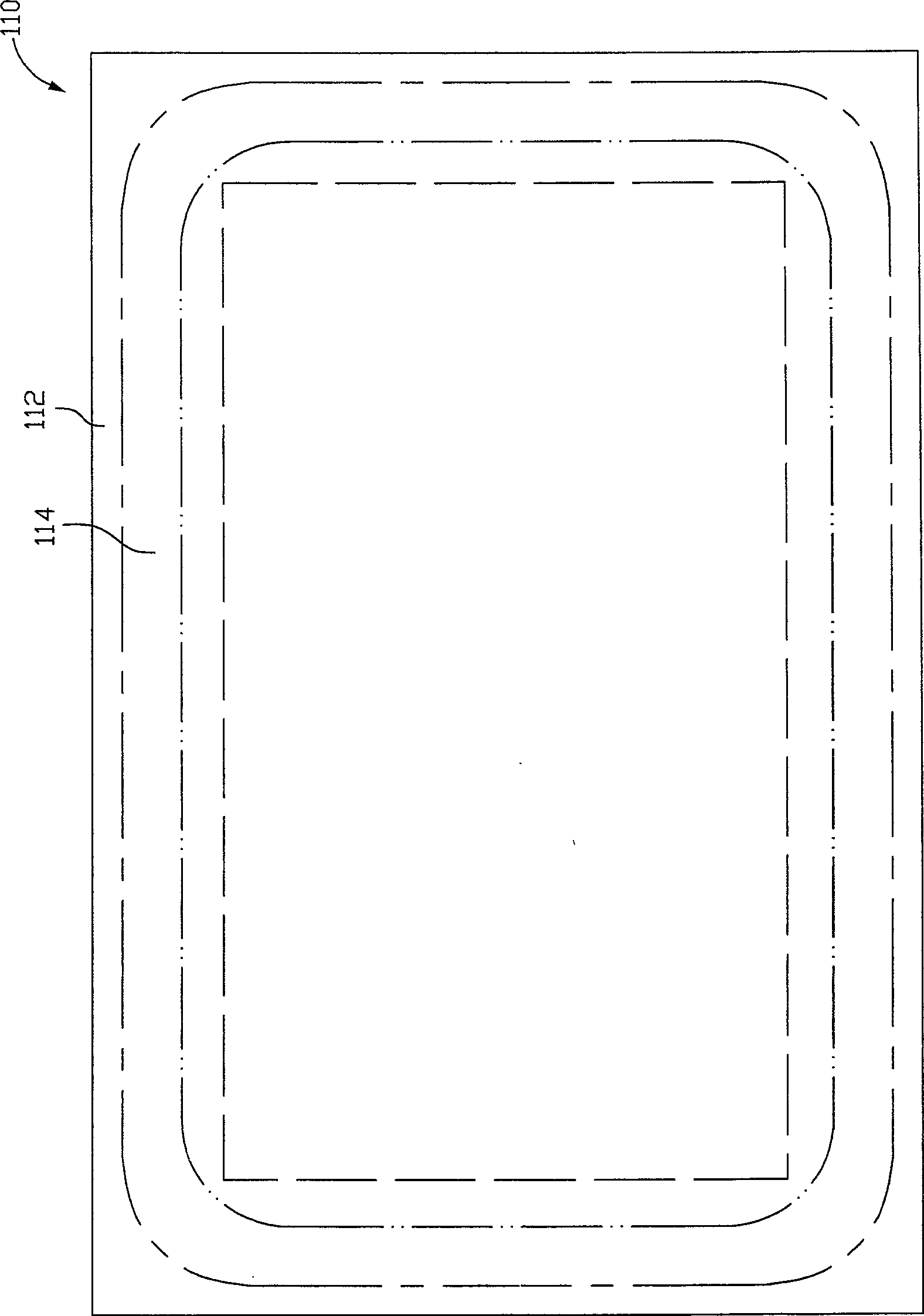
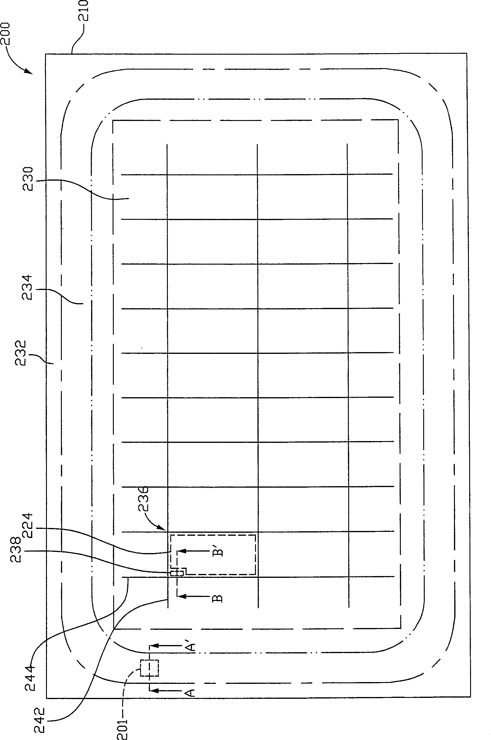
[0050] figure 2 A schematic top view of a thin film transistor array substrate according to a preferred embodiment of the present invention is shown. Please refer to figure 2, the thin film transistor array substrate 200 has a display area 230 and a non-display area 232, and includes a transparent substrate 210, a plurality of pixel units 236 and a light shielding structure 234, wherein the pixel unit 236 is arranged in the display area 230, and includes a TFT 238 and a pixel electrode 224 . The light shielding structure 234 is located in the non-display area 232 of the TFT array substrate 200 .

[0051] More specifically, the transparent substrate 210 is, for example, a glass substrate, the display area 230 is, for example, a rectangular area located in the center of the glass substrate, and the non-display area 232 is, for example, a frame-shaped area surrounding the display area 230 . A plurality of data lines 244 and scan lines 242 parallel to each other are disposed ...


PUM


Abstract

The invention discloses a thin-film transistor array substrate and a manufacturing method thereof. The thin-film transistor array substrate includes a transparent substrate, a plurality of pixel units and a light-shielding structure with a plurality of light-shielding layers. The transparent substrate has a display area and a non-display area, the pixel unit is arranged in the display area, each pixel unit includes a thin film transistor and a pixel electrode, the light-shielding layer is arranged in the non-display area and has a plurality of holes, two adjacent light-shielding The layers of holes are arranged in a staggered manner.

Description

technical field [0001] The invention relates to a liquid crystal display component, in particular to a thin film transistor array substrate and a manufacturing method thereof. Background technique [0002] The manufacture of general liquid crystal display can be roughly divided into thin film transistor array substrate manufacturing process, color filter substrate manufacturing process, liquid crystal injection and liquid crystal display module assembly. In order to prevent the light emitted by the backlight of the liquid crystal display from being scattered from the non-display area of ​​the liquid crystal display panel to the display area, a light-shielding structure is often formed in the non-display area, and the light-shielding structure is arranged around the periphery of the display area to prevent the The light leakage reduces the display quality of the display area. [0003] The light-shielding structure can be arranged on the thin film transistor array substrate, ...

Claims


Application Information

Patent Timeline
Patent Type & Authority Patents(China)
IPC IPC(8): H01L27/12H01L21/82G02F1/133
Inventor 许汉东
Owner CHUNGHWA PICTURE TUBES LTD
Why Eureka
Try Eureka