Image sensing element and manufacturing method thereof
A technology of sensing element and manufacturing method, which is applied in electrical elements, image communication, radiation control devices, etc., can solve the problem of image sensing chip being easily contaminated
- Summary
- Abstract
- Description
- Claims
- Application Information
AI Technical Summary
Problems solved by technology
Method used
Image
Examples
Embodiment Construction
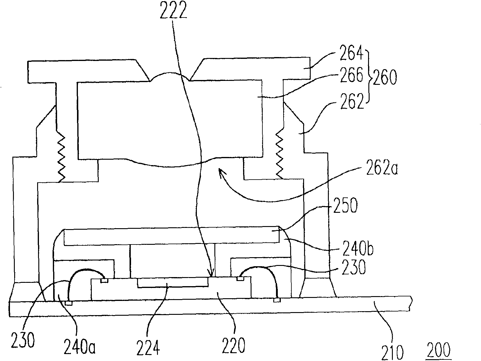
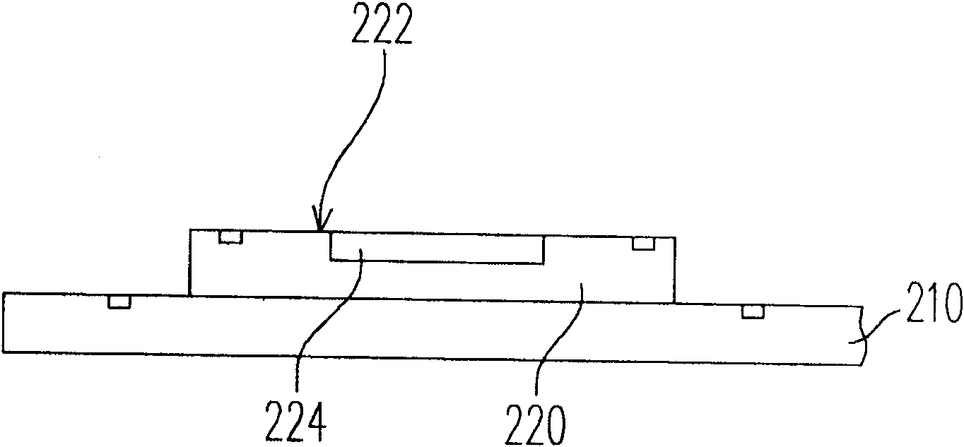
[0027] figure 2 is a schematic cross-sectional view of an image sensing element according to an embodiment of the present invention. see figure 2 The image sensor element 200 includes a circuit board 210 , an image sensor chip 220 , a plurality of wires 230 , a first annular colloid 240 a , a second annular colloid 240 b and a filter 250 . Wherein, the circuit board 210 is, for example, a flexible circuit board or a general printed circuit board (printed circuit board, PCB). The image sensor chip 220 is disposed on the circuit board 210 and has an active surface 222 away from the circuit board 210 . A plurality of wires 230 are electrically connected to the image sensor chip 220 and the circuit board 210 , and the wires 230 can be connected between the image sensor chip 220 and the circuit board 210 by wire bonding technology. The first annular glue 240 a is disposed on the circuit board 210 , surrounds the image sensor chip 220 , and covers the surrounding areas of the w...
PUM
 Abstract
Description
Claims
Application Information


