Method for manufacturing semiconductor

A manufacturing method and semiconductor technology, applied in semiconductor/solid-state device manufacturing, electrical components, circuits, etc., can solve problems such as the adverse effects of oxidized wafers, increase production costs, and consumption, so as to reduce production costs, reduce consumption, and avoid The effect of particulate matter

Active Publication Date: 2015-02-25
INST OF MICROELECTRONICS CHINESE ACAD OF SCI
View PDF4 Cites 0 Cited by
  • Summary
  • Abstract
  • Description
  • Claims
  • Application Information

AI Technical Summary

Problems solved by technology

In actual production, a large number of dummy wafers will be consumed, which increases the production cost; at the same time, the oxidation of dummy wafers may also introduce particulate matter, thereby adversely affecting the wafer 12 to be oxidized

Method used


Image

  • Method for manufacturing semiconductor
  • Method for manufacturing semiconductor
  • Method for manufacturing semiconductor

Examples


Embodiment Construction

[0017] The features and technical effects of the technical solution of the present invention will be described in detail below with reference to the accompanying drawings and in combination with exemplary embodiments.

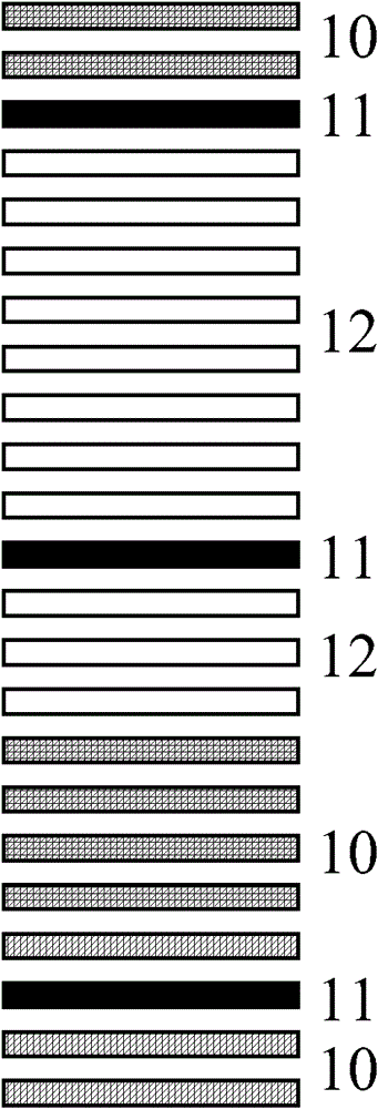
[0018] Firstly, a wafer to be oxidized 12 , a dummy wafer 10 , and a monitor wafer 11 are provided. When the wafer 12 to be oxidized does not fully occupy the thermal oxidation equipment, a certain number of dummy wafers 10 need to be placed in the thermal oxidation equipment, so that the total wafers can fill the thermal oxidation equipment as much as possible to eliminate the load effect. It can make the oxidation effect of each part of the oxidation furnace and each batch consistent, see the attached figure 1 .

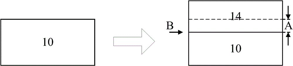
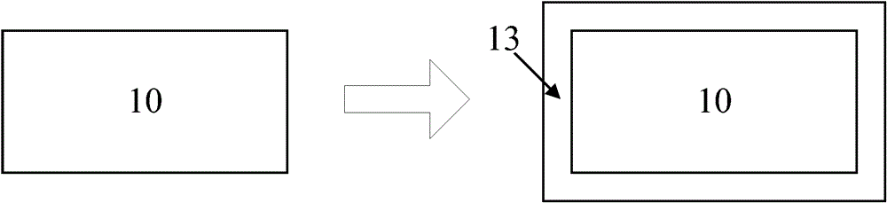
[0019] Before each wafer is put into thermal oxidation equipment for thermal oxidation process, a layer of protective film 13 is deposited on the outer surface of the dummy wafer 10, so that the protective film 13 completely covers the dummy wafer ...


PUM


Abstract

A method for manufacturing a semiconductor is provided. A layer of protective film (13) is deposited on dummy wafers (10), and the dummy wafers (10) are fully covered by the protective film (13). During a thermal oxidation process, the dummy wafers (10) can not be oxidized, thus loss of the dummy wafers can be reduced, cost of production can be decreased, and particles produced due to oxidation of the dummy wafers can be avoided, to prevent the wafers (12) to be oxidized from contamination.

Description

technical field [0001] The invention relates to a semiconductor manufacturing method, in particular to a semiconductor manufacturing method using a dummy wafer for thermal oxidation. Background technique [0002] Thermal oxidation is one of the most commonly used process steps in semiconductor manufacturing processes. Thermal oxidation is usually performed in a thermal oxidation furnace. Due to the loading effect, a dummy wafer needs to be introduced in the thermal oxidation process, which can make the uniformity of the thermal oxidation process better. See attached figure 1 , this is the wafer 12 to be oxidized, the dummy wafer 10, and the monitor wafer 11 (monitor wafer) used to manufacture semiconductor devices in the same thermal oxidation furnace. Since the wafer 12 to be oxidized does not fully occupy the thermal oxidation furnace , in order to avoid the influence of the load effect on the uniformity of oxidation, several dummy wafers 10 are introduced, so that the o...

Claims


Application Information

Patent Timeline
Patent Type & Authority Patents(China)
IPC IPC(8): H01L21/318H01L21/31
CPCH01L21/02238
Inventor 李春龙李俊峰
Owner INST OF MICROELECTRONICS CHINESE ACAD OF SCI
Why Eureka
Try Eureka