Magnetic elements with spin engineered insertion layers and MRAM devices using the magnetic elements

a technology of magnetic elements and mrams, which is applied in the field of magnetic memory systems, can solve the problems of increasing the power consumption of conventional spin transfer based mrams, adversely affecting the utility and affecting the reliability of such conventional magnetic elements, so as to reduce the size of the cell in the mram, improve reliability, and reduce power consumption.

Active Publication Date: 2008-05-06
SAMSUNG SEMICON
View PDF5 Cites 204 Cited by
  • Summary
  • Abstract
  • Description
  • Claims
  • Application Information

AI Technical Summary

Benefits of technology

[0011]According to the method and system disclosed herein, the present invention provides a magnetic element that can be written using spin transfer at a lower write current, thereby reducing power consumption, cell size in an MRAM, and improving reliability.

Problems solved by technology

Both of these features adversely affect the utility and reliability of such conventional magnetic elements 10 / 10′ in a magnetic memory.
The high write current generally required would increase the power consumption of conventional spin transfer based MRAMs.
In addition, the conventional magnetic element 10′, which has a higher resistance and thus a higher signal, may be less reliable because the conventional barrier layer 16′ may be subject to dielectric breakdown at higher write currents.
Thus, the conventional magnetic elements 10 / 10′ may be unsuitable for use in higher density conventional MRAMs using spin transfer to write to the conventional magnetic elements 10 / 10′.

Method used


Image

  • Magnetic elements with spin engineered insertion layers and MRAM devices using the magnetic elements
  • Magnetic elements with spin engineered insertion layers and MRAM devices using the magnetic elements
  • Magnetic elements with spin engineered insertion layers and MRAM devices using the magnetic elements

Examples


Embodiment Construction

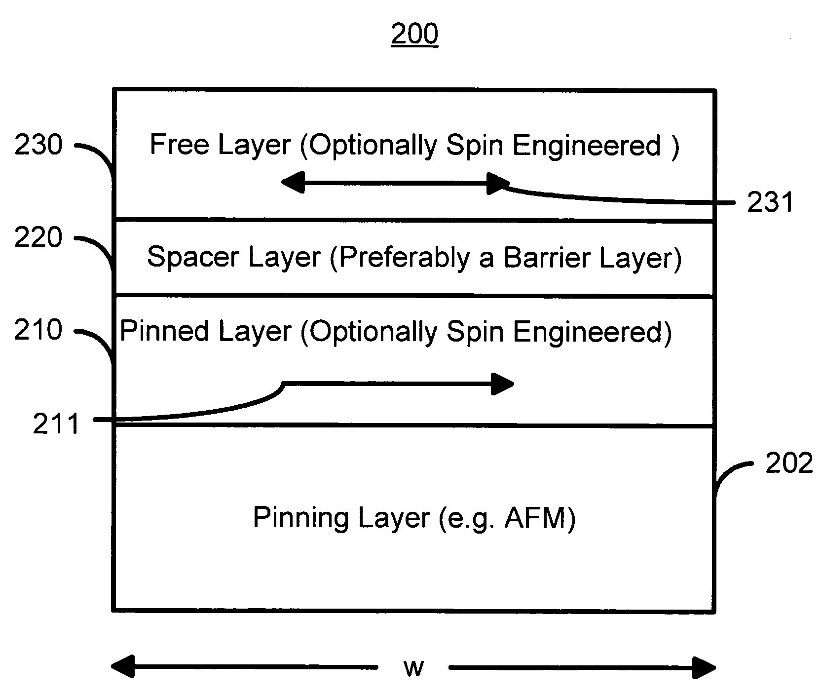
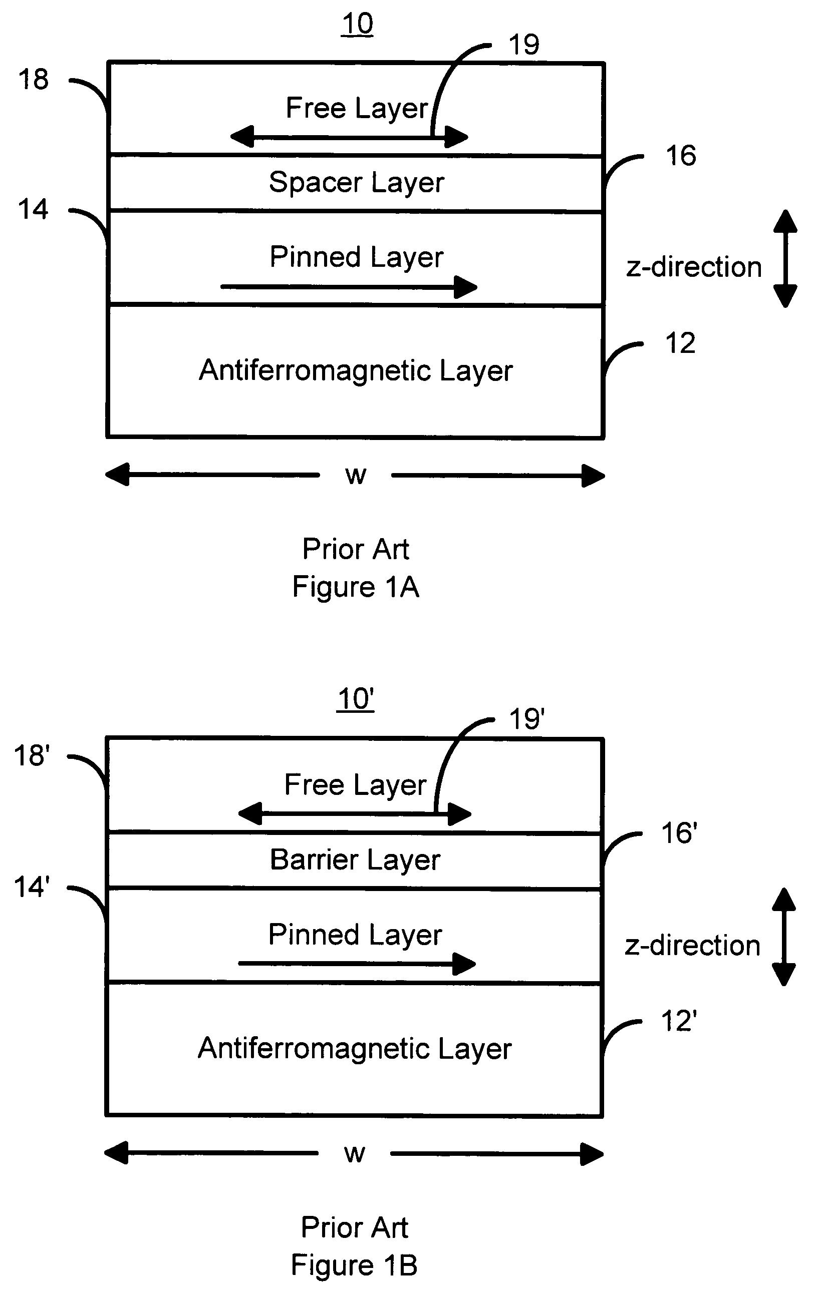
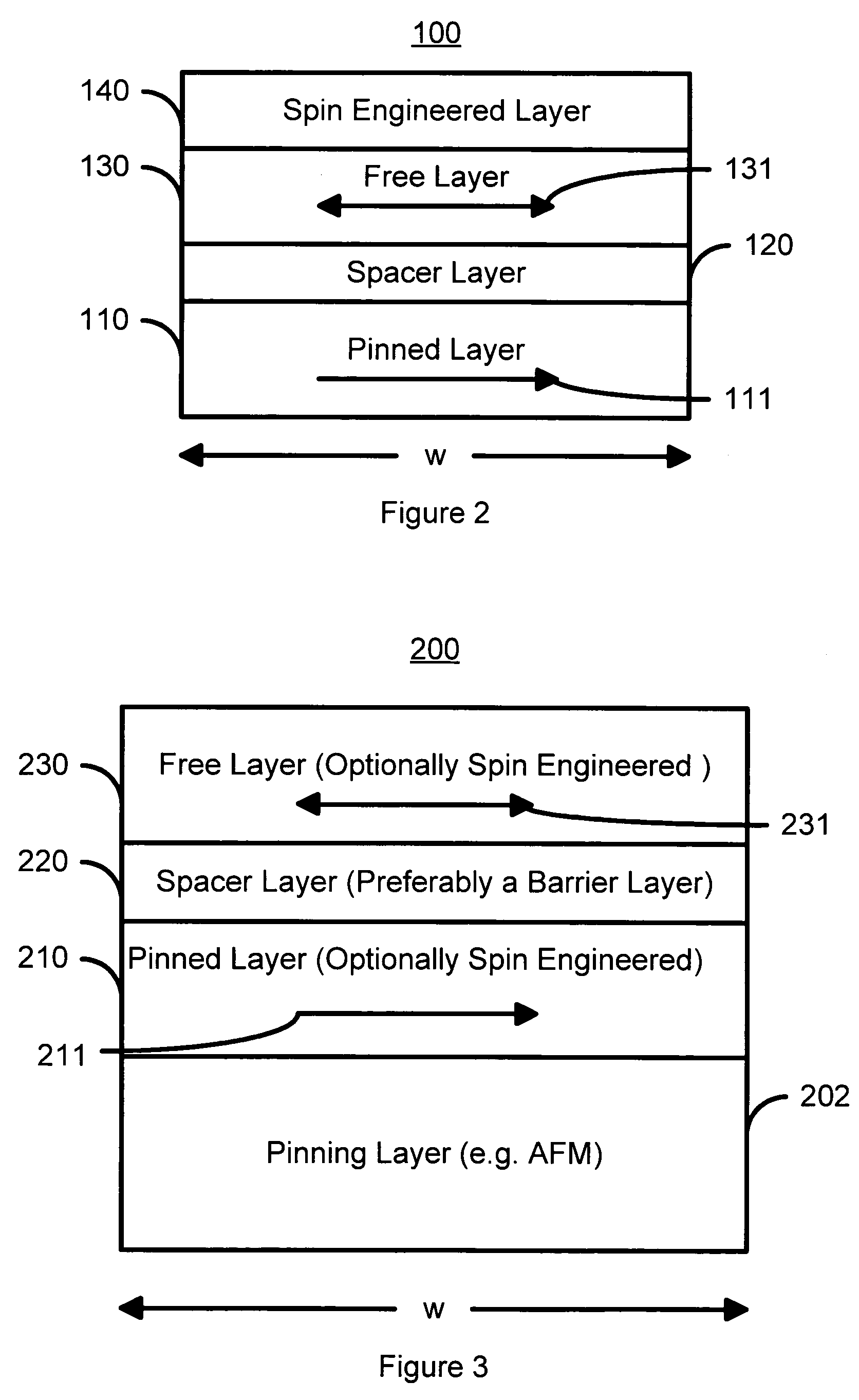
[0028]The present invention relates to magnetic elements and magnetic memories such as MRAM. The following description is presented to enable one of ordinary skill in the art to make and use the invention and is provided in the context of a patent application and its requirements. Various modifications to the preferred embodiments and the generic principles and features described herein will be readily apparent to those skilled in the art. Thus, the present invention is not intended to be limited to the embodiments shown, but is to be accorded the widest scope consistent with the principles and features described herein.

[0029]The present invention provides a method and system for providing a magnetic element. The method and system include providing a pinned layer, a free layer, and a spacer layer between the pinned and free layers. The spacey layer is nonmagnetic. The magnetic element is configured to allow the free layer to be switched due to spin transfer when a write current is p...


PUM


Abstract

A method and system include providing a pinned layer, a free layer, and a spacer layer between the pinned and free layers. The spacer layer is nonmagnetic. The magnetic element is configured to allow the free layer to be switched due to spin transfer when a write current is passed through the magnetic element. In one aspect, the method and system include providing a spin engineered layer adjacent to the free layer. The spin engineered layer is configured to more strongly scatter majority electrons than minority electrons. In another aspect, at least one of the pinned, free, and spacer layers is a spin engineered layer having an internal spin engineered layer configured to more strongly scatter majority electrons than minority electrons. In this aspect, the magnetic element may include another pinned layer and a barrier layer between the free and pinned layers.

Description

FIELD OF THE INVENTION[0001]The present invention relates to magnetic memory systems, and more particularly to a method and system for providing a magnetic element that employs a spin transfer effect in switching, that can be switched at a reduced current and that is suitable for use in a magnetic memory such as magnetic random access memory (“MRAM”).BACKGROUND OF THE INVENTION[0002]FIGS. 1A and 1B depict conventional magnetic elements 10 and 10′. The conventional magnetic element 10 is a spin valve and includes a conventional antiferromagnetic (AFM) layer 12, a conventional pinned layer 14, a conventional nonmagnetic spacer layer 16 and a conventional free layer 18. Other layers (not shown), such as seed or capping layer may also be used. The conventional pinned layer 14 and the conventional free layer 18 are ferromagnetic. Thus, the conventional free layer 18 is depicted as having a changeable magnetization 19. The conventional nonmagnetic spacer layer 16 is conductive. The AFM la...

Claims


Application Information

Patent Timeline
Patent Type & Authority Patents(United States)
IPC IPC(8): G11C11/00G11C11/14G11C11/15
CPCB82Y25/00B82Y40/00H01F10/3272H01F41/302H01L43/10H01F10/30H10N50/85
Inventor DIAO, ZHITAOHUAI, YIMINGVALET, THIERRYNGUYEN, PAUL P.PAKALA, MAHENDRA
Owner SAMSUNG SEMICON
Why Eureka
Try Eureka