Semiconductor Device And Method For Manufacturing Same

a technology of semiconductors and semiconductors, applied in the direction of semiconductor devices, basic electric elements, electrical appliances, etc., can solve the problems of comparatively high forward voltage uf, large sturdiness, and reverse current, and achieve the effects of low forward voltage, low reverse current, and great sturdiness

Active Publication Date: 2008-08-21
ROBERT BOSCH GMBH
View PDF6 Cites 165 Cited by
  • Summary
  • Abstract
  • Description
  • Claims
  • Application Information

AI Technical Summary

Benefits of technology

[0007]The present invention provides a semiconductor device having a low forward voltage, low reverse current and great sturdiness.

Problems solved by technology

Advantages of PN diodes include low reverse current and great sturdiness.
However, the main disadvantage is a comparatively high forward voltage UF.
At room temperature, current begins to flow only at a forward voltage UF of approximately 0.7 V. Under normal operating conditions at which the current density is approximately 500 A / cm2, forward voltage UF increases to more than 1 V. This results in a decline in efficiency.
Inasmuch as is known, however, Schottky diodes have not yet been used in the generator system of a motor vehicle.
This may be attributed to some significant disadvantages of a Schottky diode which make such an application appear to be less relevant.
Finally, a Schottky diode has inferior sturdiness, in particular at high temperatures.
These disadvantages have so far prevented the use of Schottky diodes in automotive applications.
More extensive screening, e.g., by an even deeper p diffusion, however, is not feasible because at the same time the diffusion region would also be extended further in the lateral direction.
However, the area available for current flow in the forward direction would then be further reduced in a deleterious manner.
Consequently, the MOS structure may be degraded from an n-epi layer to an oxide layer by injection of “hot” charge carriers and may even be destroyed under particularly adverse conditions.
This may result in brief unwanted breakdown operation of the diode.
It is therefore not very advisable to use a TMBS that has been improved with regard to the reverse current as a Z diode and operate it in the breakdown range.

Method used


Image

  • Semiconductor Device And Method For Manufacturing Same
  • Semiconductor Device And Method For Manufacturing Same
  • Semiconductor Device And Method For Manufacturing Same

Examples


Embodiment Construction

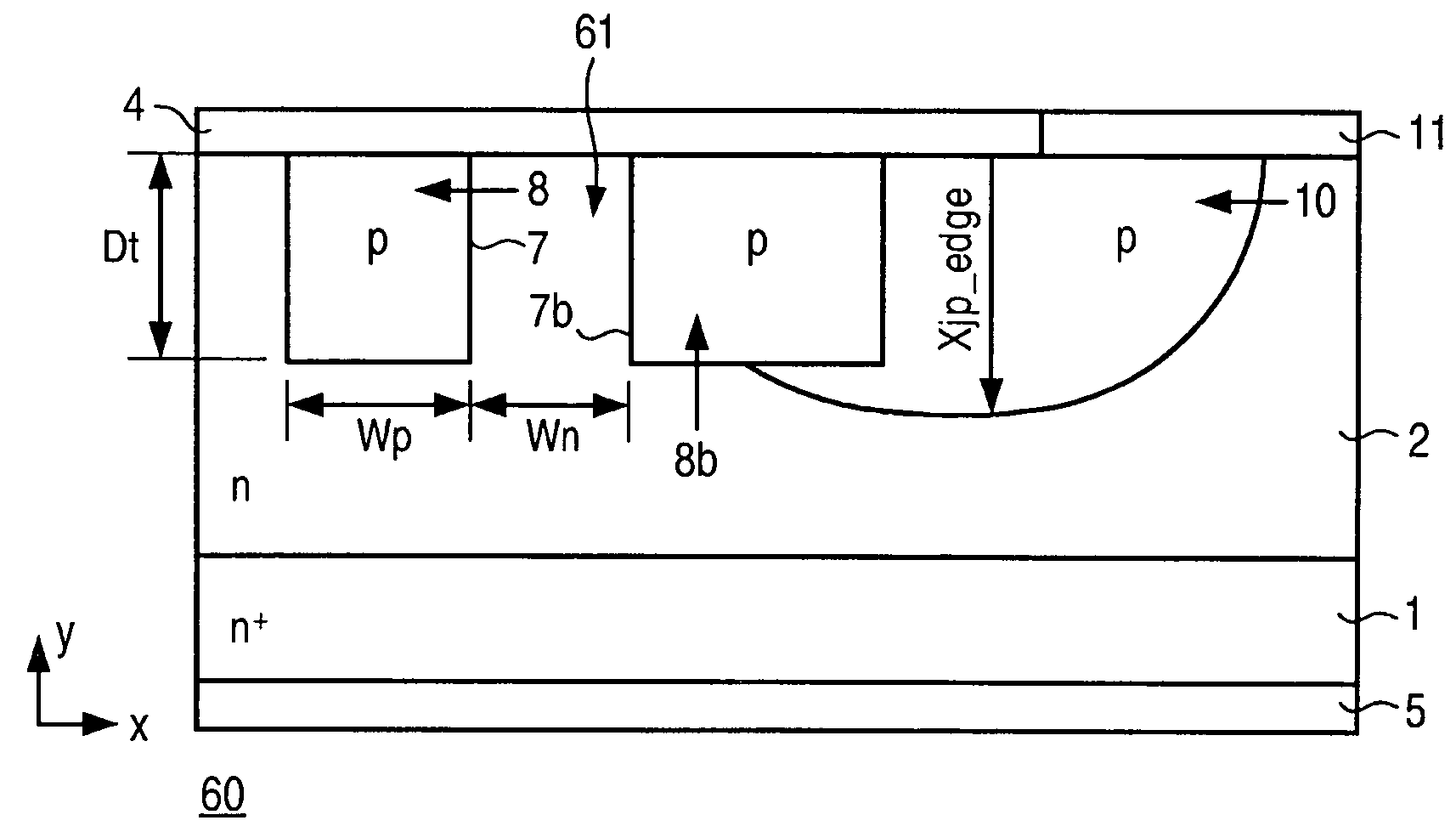
[0021]Known semiconductor devices are described briefly below to better present the advantages achievable with the present invention. FIG. 1 shows a semiconductor device 10 in the form of a traditional JBS (junction-barrier Schottky diode), which includes an n+ substrate 1, an n-layer 2, at least two p troughs 3 that have diffused into n-layer 2 and contact layers 4 and 5 on the front and back sides of the chip. Electrically, a JBS is a combination of a PN diode (PN junction between p troughs 3 as the anode and n-layer 2 as the cathode) and a Schottky diode (Schottky barrier between contact layer 4 as the anode and n-layer 2 as the cathode). Contact layer 5 on the back side of the chip functions as the cathode, while contact layer 4 on the front side of the chip functions as the anode with ohmic contact to p troughs 3 and at the same time functions as a Schottky contact to n-layer 2. Because of the low forward voltage of the Schottky diode in comparison with the PN diode, a current ...


PUM


Abstract

A semiconductor device including a Schottky diode of the trench-junction-barrier type having an integrated PN diode, and a corresponding method for manufacturing the device, are provided. An n layer is provided on an nt substrate, and trenches are provided in the n layer. The trenches are provided with p-doped regions. The nt substrate and the n layer carry a contact layer.

Description

BACKGROUND OF THE INVENTION[0001]1. Field of the Invention[0002]The present invention relates to a semiconductor device which is a junction-barrier Schottky diode having a trench structure, which semiconductor device is suitable as a Z diode (Zener diode) for use in the electrical system of a motor vehicle.[0003]2. Description of Related Art[0004]In modern motor vehicles, more and more functions are being implemented using electrical components. This results in an ever-increasing demand for electric power. To meet this demand, the efficiency of the generator system in the motor vehicle must be increased. So far, PN diodes have been usually used as Z diodes in the generator system of the motor vehicle. Advantages of PN diodes include low reverse current and great sturdiness. However, the main disadvantage is a comparatively high forward voltage UF. At room temperature, current begins to flow only at a forward voltage UF of approximately 0.7 V. Under normal operating conditions at whi...

Claims


Application Information

Patent Timeline
Patent Type & Authority Applications(United States)
IPC IPC(8): H01L29/872H01L29/861H01L21/329H01L29/866
CPCH01L29/8611H01L29/8725H01L29/66143H01L29/872H01L29/0619H01L21/18H01L29/866H01L29/861
Inventor GOERLACH, ALFREDQU, NING
Owner ROBERT BOSCH GMBH
Why Eureka
Try Eureka