

Flip chip nitride semiconductor light emitting diode
一种氮化物半导体、发光二极管的技术,应用在半导体器件、管子、管元件等方向,能够解决增加正向电压、降低发光效率、低特殊电阻等问题
- Summary
- Abstract
- Description
- Claims
- Application Information
AI Technical Summary
Problems solved by technology
Method used
Image

Examples
example 1
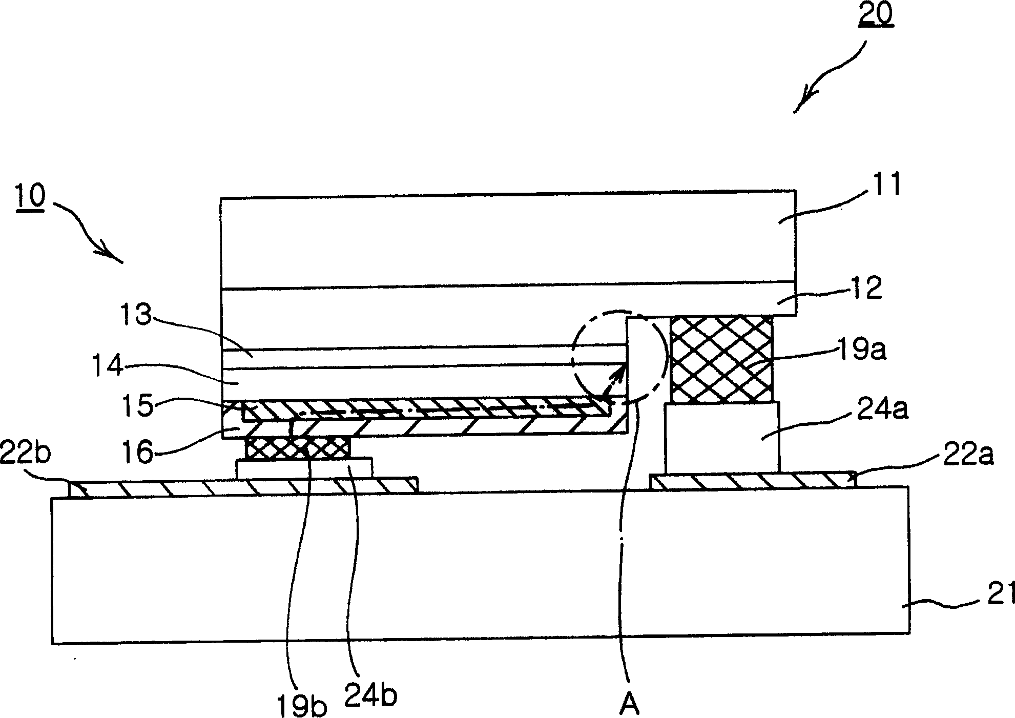
[0076] First, after loading the sapphire substrate into the MOCVD chamber, a GaN low-temperature nucleation layer is grown as a buffer layer. Then, an n-doped semiconductor layer of an n-doped GaN film and an n-doped AlGaN layer, an active layer having a plurality of quantum well structures of InGaN / GaN films, and a p-doped GaN film are formed on the buffer layer p-doped nitride semiconductor layer to obtain blue LED.
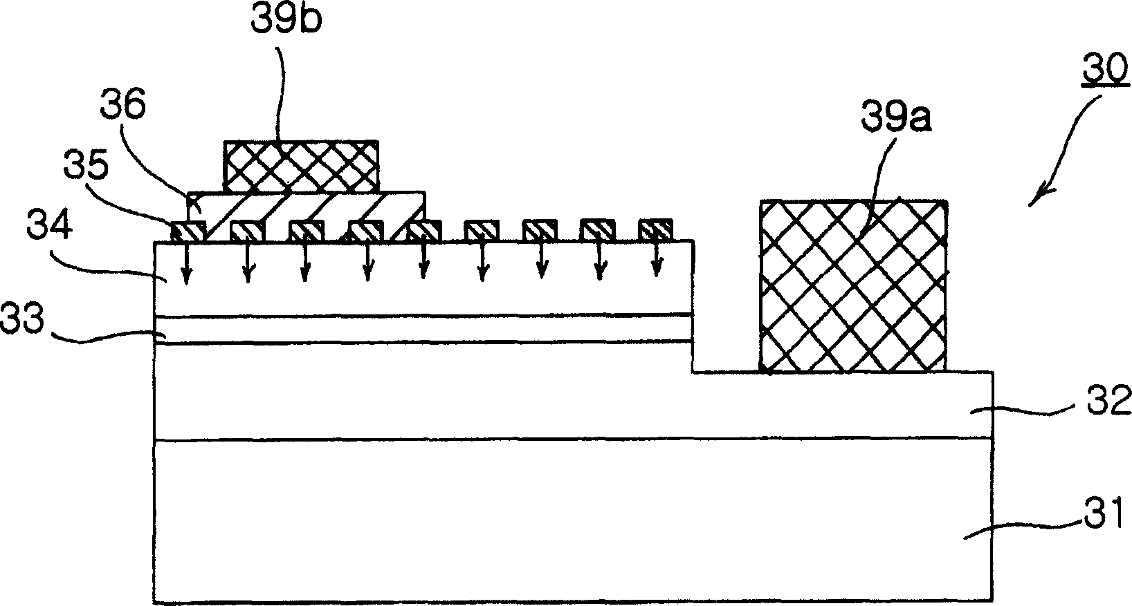
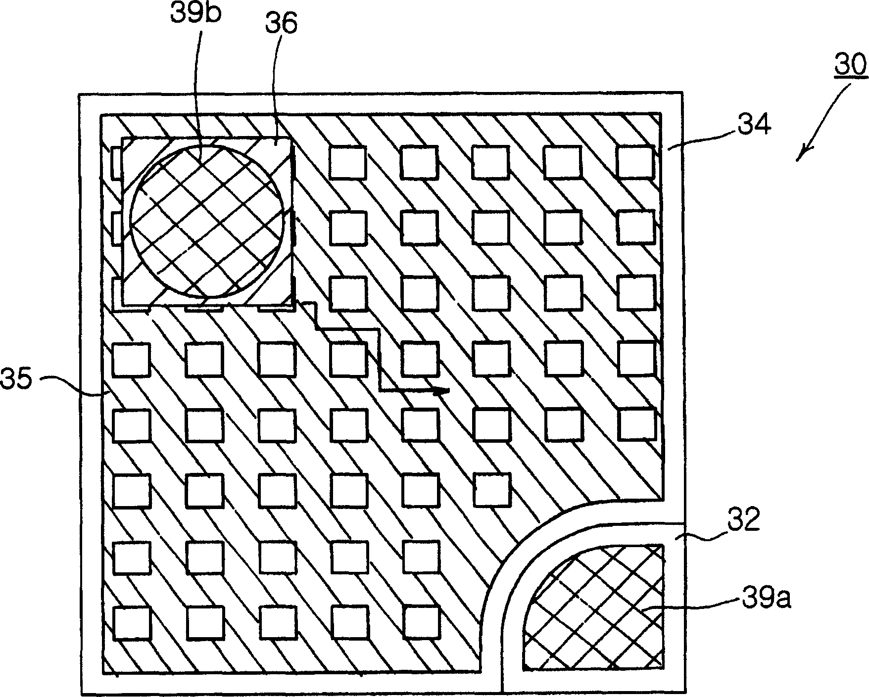
[0077] Next, a high-reflectivity ohmic contact layer having a network structure with an opening area ratio of about 30% was formed on the p-doped nitride semiconductor layer, and the resulting structure was then heat-treated at a temperature of about 500°C. The high-reflectivity ohmic contact layer of Inventive Example 1 was made of Ni / Ag. Here, the opening area ratio means the ratio of the opening area to the entire area (ie, the area surrounded by the outermost periphery), as generally used in this specification.
[0078] Then, a metal barrier layer is form...
example 2
[0081] In Invention Example 2, a flip-chip nitride semiconductor LED was fabricated according to the same conditions as Invention Example 1, except that the high-reflectivity ohmic contact layer of the mesh structure was patterned to have an opening area ratio of about 50%. The thus prepared flip-chip nitride semiconductor LED is connected to a supporting substrate having a lead pattern such as Figure 3B As shown, a flip-chip light-emitting device was produced.
example 3
[0083] In Inventive Example 3, a flip-chip nitride semiconductor LED was fabricated according to the same conditions as Inventive Example 1, except that the high-reflectivity ohmic contact layer of the mesh structure was patterned to have an opening area ratio of about 70%. The thus prepared flip-chip nitride semiconductor LED is connected to a supporting substrate having a lead pattern such as Figure 3B As shown, a flip-chip light-emitting device was produced.
[0084] comparison example
[0085] In the comparative example, flip-chip nitride semiconductor LEDs were prepared according to the same conditions as Inventive Examples 1 to 3, except for a high-reflectivity ohmic contact layer formed in a conventional structure with the same entire area, without a separate mesh structure. composition process. The thus prepared flip-chip nitride semiconductor LED is connected to a supporting substrate having a lead pattern such as Figure 3B As shown, a flip-chip light-emitting de...
PUM
 Abstract
Description
Claims
Application Information