N-Type Group III Nitride Semiconductor Layered Structure

a layered structure and nitride technology, applied in semiconductor/solid-state device manufacturing, semiconductor devices, electrical equipment, etc., can solve the problems of low resistance and continuous nitride semiconductor layers that have not been reliably obtained, emission intensity is lowered after aging, and the layer is prone to cracks. , to achieve the effect of low forward voltage, low resistance and high flatness

Inactive Publication Date: 2008-09-25
TOYODA GOSEI CO LTD
View PDF5 Cites 17 Cited by
  • Summary
  • Abstract
  • Description
  • Claims
  • Application Information

AI Technical Summary

Benefits of technology

[0011]An object of the present invention is to provide a low-resistance n-type Group III nitride semiconductor layered structure having excellent flatness and few pits. Another object of the invention is to provide, from the semiconductor layered structure, a Group III nitride semiconductor light-emitting device exhibiting low forward voltage and high emission efficiency.
[0012]Further, another object of the invention is to Provide a group III nitride semiconductor light-emitting device in which light emission characteristics are excellent and a change in characteristics such as a lowering in emission intensity and a reduction in peak inverse voltage caused by aging is very small.
[0014]The n-type Group III nitride semiconductor layered structure of the present invention exhibits low resistance and high flatness, since pits formed in the low-resistive n-type impurity atom higher concentration layer are filled up with a portion of the n-type impurity atom lower concentration layer. Therefore, the light-emitting device of the present invention including such an n-type Group III nitride semiconductor layered structure exhibits low forward voltage and excellent emission efficiency.
[0015]The utilization of the n-type group III nitride semiconductor layered structure according to the present invention in the n-type contact layer in the light-emitting device is particularly effective. Specifically, this is advantageous in that the resistance is low and, at the same time, as compared with the case where film formation is carried out with doping without providing any concentration difference, the surface flatness is superior and, thus, the crystallinity of the light-emitting layer overlying the film is not deteriorated. Further, fine pit formation on the dried etched surface lowers the resistance of contact with the electrode.
[0016]Further, according to the present invention, a group III nitride semiconductor light-emitting device is provided in which light emission characteristics are excellent and a change in characteristics such as a lowering in emission intensity and a reduction in peak inverse voltage caused by aging is very small.

Problems solved by technology

However, when a large amount of silicon is added during vapor growth of a low-resistive n-type Group III nitride semiconductor layer, problematic cracks are generated in the layer.
In other words, even when conventional technical means; i.e., doping with silicon, is employed, a low-resistive and continuous n-type Group III nitride semiconductor layer has not been reliably obtained.
An LED in which Si has been doped into the n-type layer, however, has a problem that, due to the movement of Si within the semiconductor crystal by energization for a long period of time, the emission intensity is lowered after aging.
The highly efficient LED described in the above Japanese Patent No. 3383242 suffers from the same problems.
As compared with silicon, germanium (Ge) has poor doping efficiency and, therefore, use of germanium as a dopant is disadvantageous for producing a low-resistive n-type Group III nitride semiconductor layer.
When Ge is added in a high concentration so as to produce a low-resistive n-type Group III nitride semiconductor layer, pits that impair flatness of the surface of the n-type Group III nitride semiconductor layer are generated, which is problematic.
When the angle of inclination of the surface of the substrate is simply brought to not more than 5 degrees, as the step density of the surface of the substrate is not satisfactorily specified, the problem of nonuniform dopant distribution and the problem of lowered surface flatness cannot be solved.

Method used


Image

  • N-Type Group III Nitride Semiconductor Layered Structure
  • N-Type Group III Nitride Semiconductor Layered Structure
  • N-Type Group III Nitride Semiconductor Layered Structure

Examples


example 1

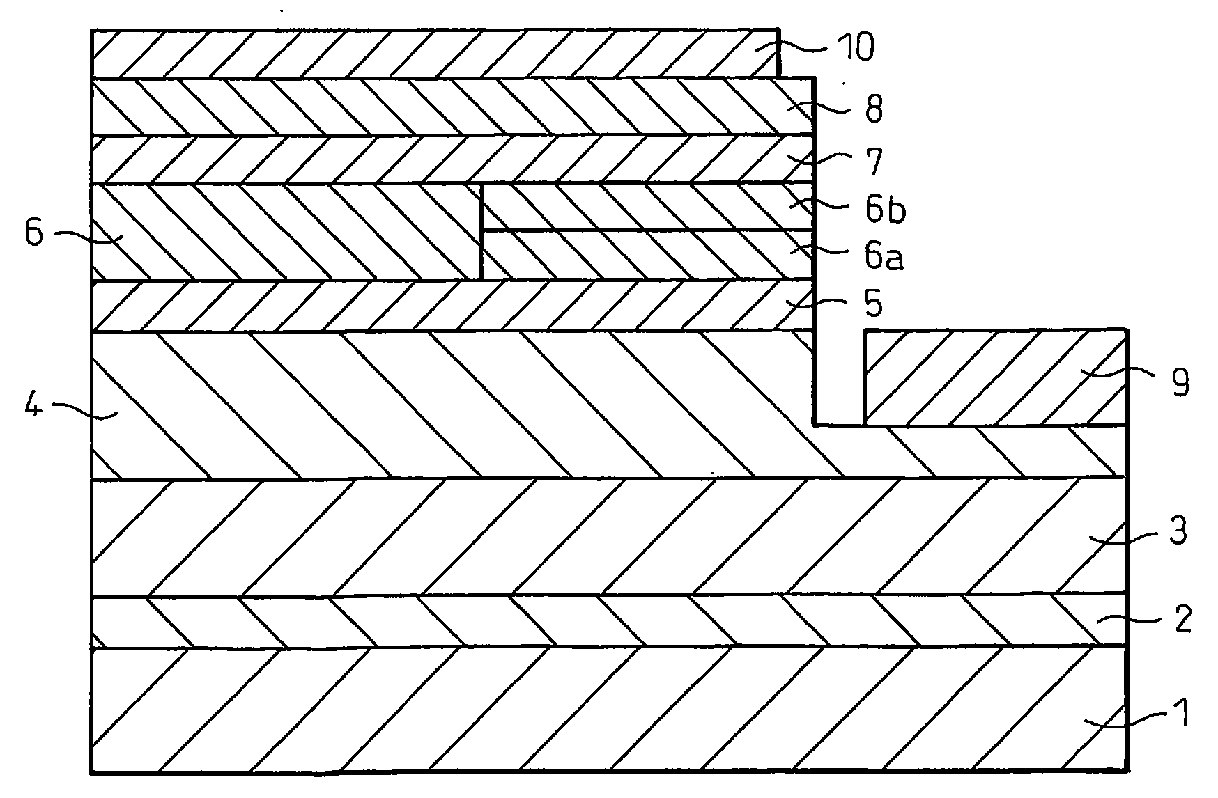
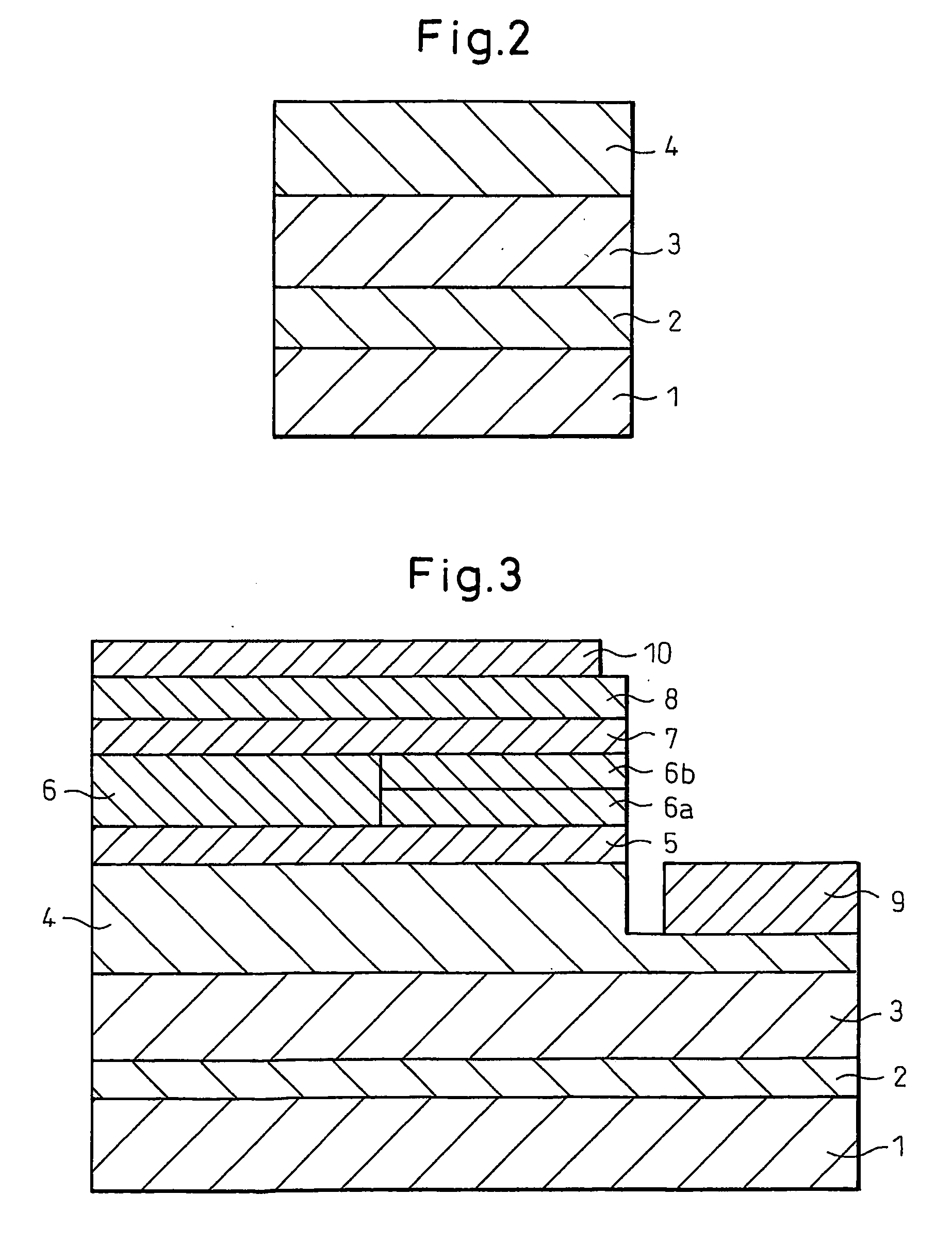
[0078]FIG. 2 schematically shows a cross-section of a stacked structure containing a Ge-doped n-type Group III nitride semiconductor layer fabricated in Example 1.

[0079]A stacked structure including a sapphire substrate and Group III nitride semiconductor layers successively stacked on the substrate was formed by means of conventional reduced-pressure MOCVD through the following procedure. Firstly, a (0001)-sapphire substrate 1 was placed on a high-purity graphite (for semiconductor) susceptor to be heated at a film formation temperature by a high-frequency (RF) induction heater. The sapphire substrate placed on the susceptor was placed in a stainless steel-made vapor growth reactor furnace, and the reactor furnace was purged with nitrogen.

[0080]After passage of nitrogen in the vapor growth reactor furnace for 8 minutes, the substrate 1 was heated over 10 minutes from room temperature to 600° C. by means of the induction heater. While the substrate 1 was maintained at 600° C., hydro...

example 2

[0088]The procedure of Example 1 was repeated, except that a plane direction of a surface of a sapphire substrate was inclined from a direction to a direction (an inclination angle: 0.35 degree), to thereby form a stacked structure.

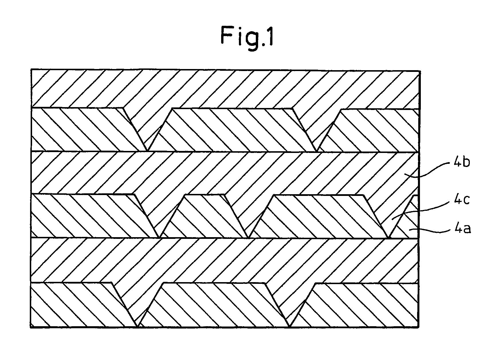
[0089]The Ge-doped n-type GaN layer 4 of the thus-produced stacked structure was found to have a carrier concentration, as measured on the basis of Hall effect, of 7×1018 cm−3, which is equivalent to that obtained in Example 1. The n-type GaN layer 4 had a remarkably flat surface having a pit density of 180 / cm2 or less. Also, a sample separately taken out from the furnace after the growth of the higher concentration layer was observed under an atomic force microscope. As a result, it was found that the density of pits produced on the surface of the higher concentration layer was 1×10⁷ / cm2.

example 3

[0090]The procedure of Example 1 was repeated, except that a Ge-doped n-type GaN layer 4 having a thickness of 2.0 μm was formed through supplying (CH3)4Ge for 9 seconds, followed by stopping supply for 9 seconds, and repeating the cycle 200 times, to thereby form a stacked structure.

[0091]The Ge-doped n-type GaN layer 4 of the thus-produced stacked structure was found to have a carrier concentration, as measured on the basis of Hall effect, of 7×1018 cm−3, which is equivalent to that obtained in Example 1. Through SIMS analysis, each higher concentration layer was found to have a Ge atom concentration of 1.2×1019 cm−3 and a thickness of 5 nm, and each lower concentration layer was found to have a Ge atom concentration of 1×1018 cm−3 and a thickness of 5 nm. The n-type GaN layer 4 had a surface having a pit density of 4,000 / cm2. Although the pit density is slightly higher than that obtained in Example 1, the surface was very flat as compared with a conventional Ge-doped n-type semic...


PUM

PropertyMeasurementUnit
Raaaaaaaaaaa
thicknessaaaaaaaaaa
thicknessaaaaaaaaaa

Abstract

An object of the present invention is to provide a low-resistance n-type Group III nitride semiconductor layered structure having excellent flatness and few pits. The inventive n-type group III nitride semiconductor layered structure comprises a substrate and, stacked on the substrate, an n-type impurity concentration periodic variation layer comprising an n-type impurity atom higher concentration layer and an n-type impurity atom lower concentration layer, said lower concentration layer being stacked on said higher concentration layer.

Description

CROSS REFERENCE TO RELATED APPLICATIONS[0001]This application is an application filed under 35 U.S.C. §111(a) claiming benefit, pursuant to 35 U.S.C. §119(e)(1), of the filing date of the Provisional Application No. 60 / 570,135 filed on May 12, 2004 and of the Provisional Application No. 60 / 585,919 filed on Jul. 8, 2004, pursuant to 35 U.S.C. §111(b).TECHNICAL FIELD[0002]The present invention relates to a n-type Group III nitride semiconductor layered structure which has, for example, germanium (Ge) as an n-type dopant and to a Group III nitride semiconductor light-emitting device including the semiconductor layered structure.BACKGROUND ART[0003]Conventionally, a Group III nitride semiconductor formed on a substrate has been used as a functional material for fabricating pn-junction Group III nitride semiconductor light-emitting devices which emit visible light of short wavelength such as light-emitting diodes (LEDs) and laser diodes (LDs) (see, for example, Japanese Patent Applicatio...

Claims


Application Information

Patent Timeline
Patent Type & Authority Applications(United States)
IPC IPC(8): H01L33/00H01L29/22H01L21/205H01L21/20H01L33/02H01L33/32
CPCH01L21/0237H01L21/0242H01L21/02433H01L21/02538H01L33/32H01L21/02576H01L21/02579H01L21/0262H01L33/025H01L21/0254
Inventor BANDOH, AKIRASAKAI, HIROMITSUKOBAYAKAWA, MASATOOKUYAMA, MINEOTOMOZAWA, HIDEKIMIKI, HISAYUKIGAZE, JOSEPHHORIKAWA, SYUNJISAKURAI, TETSUO
Owner TOYODA GOSEI CO LTD
Why Eureka
Try Eureka