Semiconductor light emitting device

a technology of light-emitting devices and semiconductors, which is applied in the direction of semiconductor devices, basic electric elements, electrical appliances, etc., can solve the problems of low light-emitting efficiency, significant deterioration of light-emitting efficiency, and the inability of reflective films containing metals with high reflectance such as au, al, and ag to be joined by ohmic, so as to achieve excellent reliability and reduce forward voltage.

Inactive Publication Date: 2009-07-21
SUMITOMO CHEM CO LTD
View PDF2 Cites 17 Cited by
  • Summary
  • Abstract
  • Description
  • Claims
  • Application Information

AI Technical Summary

Benefits of technology

[0018]Accordingly, so as to solve the above problem, it is an object of the present invention to provide a semiconductor light emitting device, in which the forward voltage can be reduced while keeping the light output and which is excellent in the reliability.
[0047]According to the present invention, it is possible to provide a semiconductor light emitting device, in which the forward voltage can be reduced while keeping the light output and which is excellent in the reliability.

Problems solved by technology

However, the light extract efficiency from the light emitting device to the outside is still low, and enhancement of the light extract efficiency is important.
Since a bandgap of the GaAs substrate is narrower than that of the active layer in such a semiconductor light emitting device, most of the light emitted from the active layer is absorbed by the GaAs substrate, so that the light extract efficiency is significantly deteriorated.
However, according to this technique, only the light having a limited incident angle with respect to the multilayer reflective film structure layer is reflected.
In addition, the reflective film comprising a metal having a high reflectance such Au, Al, and Ag cannot be joined by ohmic-contact with an AlGaInP based semiconductor.
However, in case of using the Zn based material, a forward voltage cannot be reduced enough.
In other words, there is a disadvantage in that deterioration of a light output is involved when the heat treatment temperature is elevated to reduce the forward voltage.
However, according to conventional semiconductor light emitting device using the Be based material for the ohmic contact portion, there is a disadvantage in that the light output is low and a reliability of the device is low, although the forward voltage can be reduced compared with the semiconductor light emitting device using the Zn based material for the ohmic contact portion.
In other words, it is difficult to reduce the forward voltage while keeping the light output.
This problem is a big issue for providing a higher output of the semiconductor light emitting device in future.

Method used


Image

  • Semiconductor light emitting device
  • Semiconductor light emitting device
  • Semiconductor light emitting device

Examples


example 1

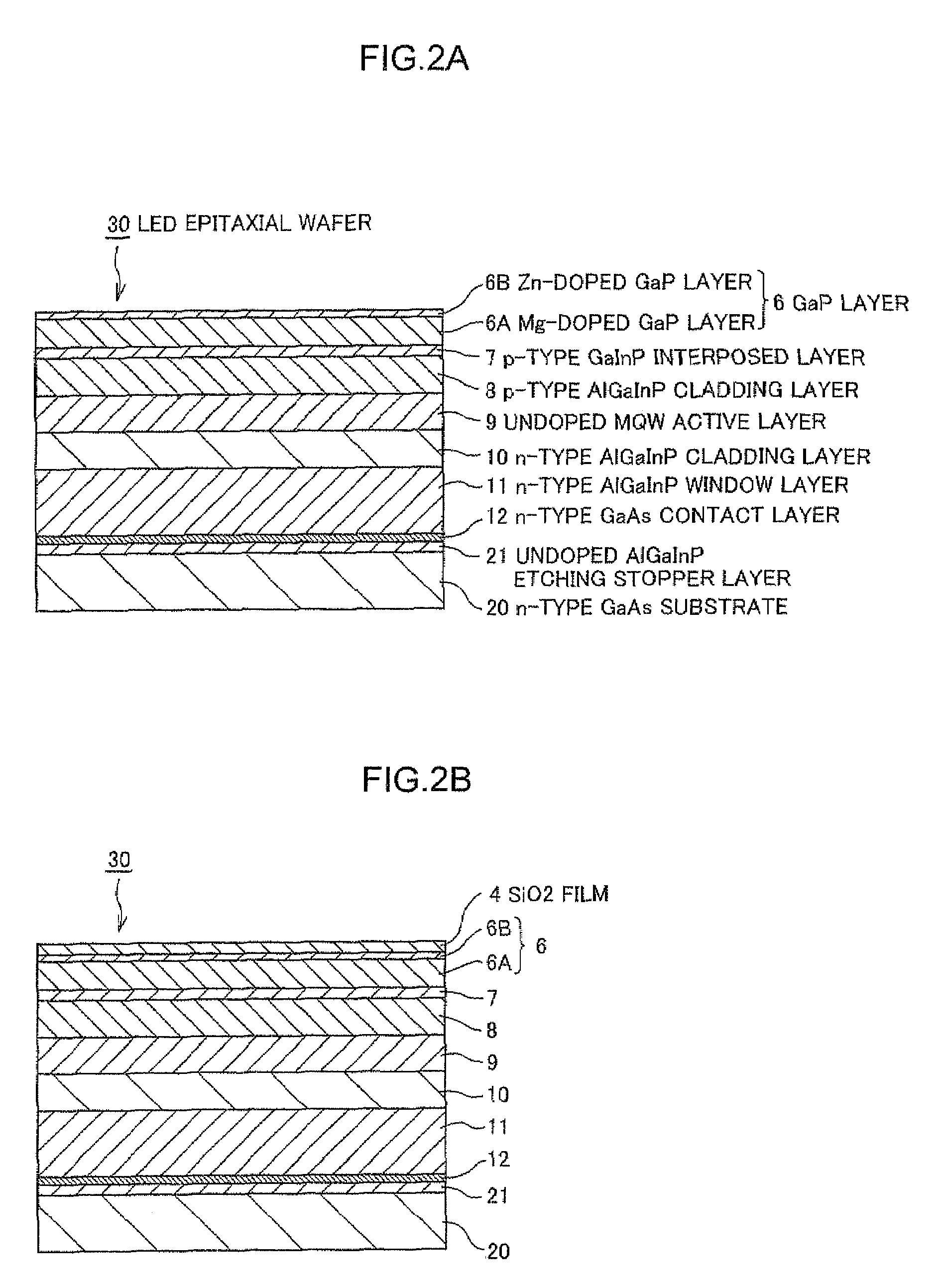
[0101]FIG. 8 is a schematic cross sectional view of a LED epitaxial wafer in Example 1 according to the present invention.

[0102]The LED epitaxial wafer 30 shown in FIG. 8 is cut by using a dicing apparatus, to provide an LED bare chip with dimensions of 300 μm×300 μm. The LED bare chip is used for a red semiconductor light emitting device with an emitting light wavelength of about 630 nm. The LED epitaxial wafer 30 shown in FIG. 8 is partially different in structure from the LED epitaxial wafer in the comparative example.

[0103]In the Example 1, the conductive material composing the ohmic contact portion 5A of the LED epitaxial wafer 30 is changed. In concrete, an AuBe ohmic contact portion 5A using an AuBe alloy in place of AuZn alloy is formed. In addition, a thickness of the GaP layer 6A is increased to be 250 nm, and a thickness of the GaP layer 6B is the same, namely 50 nm.

[0104]In other words, the Example 1 is different from the comparative example, in that a total thickness of...

example 2

[0108]FIG. 9 is a schematic cross sectional view of a LED epitaxial wafer in Example 2 according to the present invention.

[0109]The LED epitaxial wafer 30 shown in FIG. 9 is cut by using a dicing apparatus, to provide an LED bare chip with dimensions of 300 μm×300 μm. The LED bare chip is used for a red semiconductor light emitting device with an emitting light wavelength of about 630 nm. The LED epitaxial wafer 30 shown in FIG. 9 is partially different in structure from the LED epitaxial wafer in the Example 1.

[0110]In the Example 2, the AuBe ohmic contact portion 5A using an AuBe alloy is provided. In addition, a thickness of the GaP layer 6A is reduced to be 100 nm, and an undoped GaP layer 6C is provided as a third layer which is not positively doped between the GaP layer 6A and the GaP layer 6B. A total thickness of the GaP layer 6A, the GaP layer 6B, and the undoped GaP layer 6C is 300 nm.

[0111]The LED epitaxial wafer 30 thus manufactured is stuck to the Si substrate, and the ...

example 3

[0117]In Example 3, the ohmic contact portion 5A of the LED epitaxial wafer 30 comprises a AuBe based material. In the Example 3, Ti / AuBe, AuBe / Ti / AuBe, AuBe / Ti, and Ni / AuBe, doped with Ti and Ni that are transition metals, are used as the AuBe based material. Then, four kinds of wafers comprising the AuBe based material ohmic contact portion 5 were prepared.

[0118]The LED epitaxial wafer 30 thus manufactured is stuck to the Si substrate, and the LED epitaxial wafer 30 is cut similarly to the aforementioned manner, to provide a semiconductor light emitting device. The semiconductor light emitting device is mounted on a TO-18 stem to provide an LED device.

[0119]The initial characteristics and the reliability of the LED device in the Example 3 were evaluated. In all of the four kinds of the LED devices, the characteristics similar to the Example 2 are obtained.

[0120]As described above, it is observed that relative output and the reliability are improved and that the forward voltage is ...


PUM


Abstract

A Si substrate 1, a metal adhesion layer 2, a reflective metal film 3 comprising a multilayer of metallic material having a light reflectivity, a SiO2 film 4, an ohmic contact portion 5 provided at a predetermined position of the SiO2 film 4, a GaP layer 6 including a Mg-doped GaP layer 6A and a Zn-doped GaP layer 6B, a p-type GaInP interposed layer 7, a p-type AlGaInP cladding layer 8, an undoped MQW active layer 9, an n-type AlGaInP cladding layer 10, an n-type AlGaInP window layer 11, an n-type GaAs contact layer 12, a first electrode 13, and a second electrode 14 are formed. The ohmic contact portion 5 is distant from the light emitting part including the p-type AlGaInP cladding layer 8, the undoped MQW active layer 9 and the n-type AlGaInP cladding layer 10 by not less than 300 nm.

Description

[0001]The present application is based on Japanese Patent Application No. 2007-129051 filed on May 15, 2007, the entire contents of which are incorporated herein by reference.BACKGROUND OF THE INVENTION[0002]1. Field of the Invention[0003]The present invention relates to a semiconductor light emitting device, in more particular, to a high luminance type semiconductor light emitting device.[0004]2. Related Art[0005]As to a light emitting diode (LED) which is a semiconductor light emitting device, it is possible to fabricate a high luminance LED emitting various color lights such as blue, green, orange, yellow, and red, since it is possible to grow a GaN based high quality crystal or an AlGaInP based high quality crystal by using MOVPE (Metal Organic Vapor Phase Epitaxy) method in recent years. In accordance with the provision of a high luminance LED, applications of the LED are widened, e.g. a back light of a liquid crystal display, a brake lump for a vehicle so that demand for the L...

Claims


Application Information

Patent Timeline
Patent Type & Authority Patents(United States)
IPC IPC(8): H01L33/00H01L33/06H01L33/10H01L33/14H01L33/30H01L33/40
CPCH01L33/0079H01L33/14H01L33/46H01L33/0093
Inventor KONNO, TAICHIROO
Owner SUMITOMO CHEM CO LTD
Why Eureka
Try Eureka