

Magnetic tunnel junction magnetic device, memory and writing and reading methods using said device
a magnetic device and tunnel junction technology, applied in the direction of magnetic bodies, instruments, substrate/intermediate layers, etc., can solve the problems of increasing the number of addressing errors, increasing the electricity consumption, and increasing the valu
- Summary
- Abstract
- Description
- Claims
- Application Information
AI Technical Summary
Benefits of technology
Problems solved by technology
Method used
Image

Examples
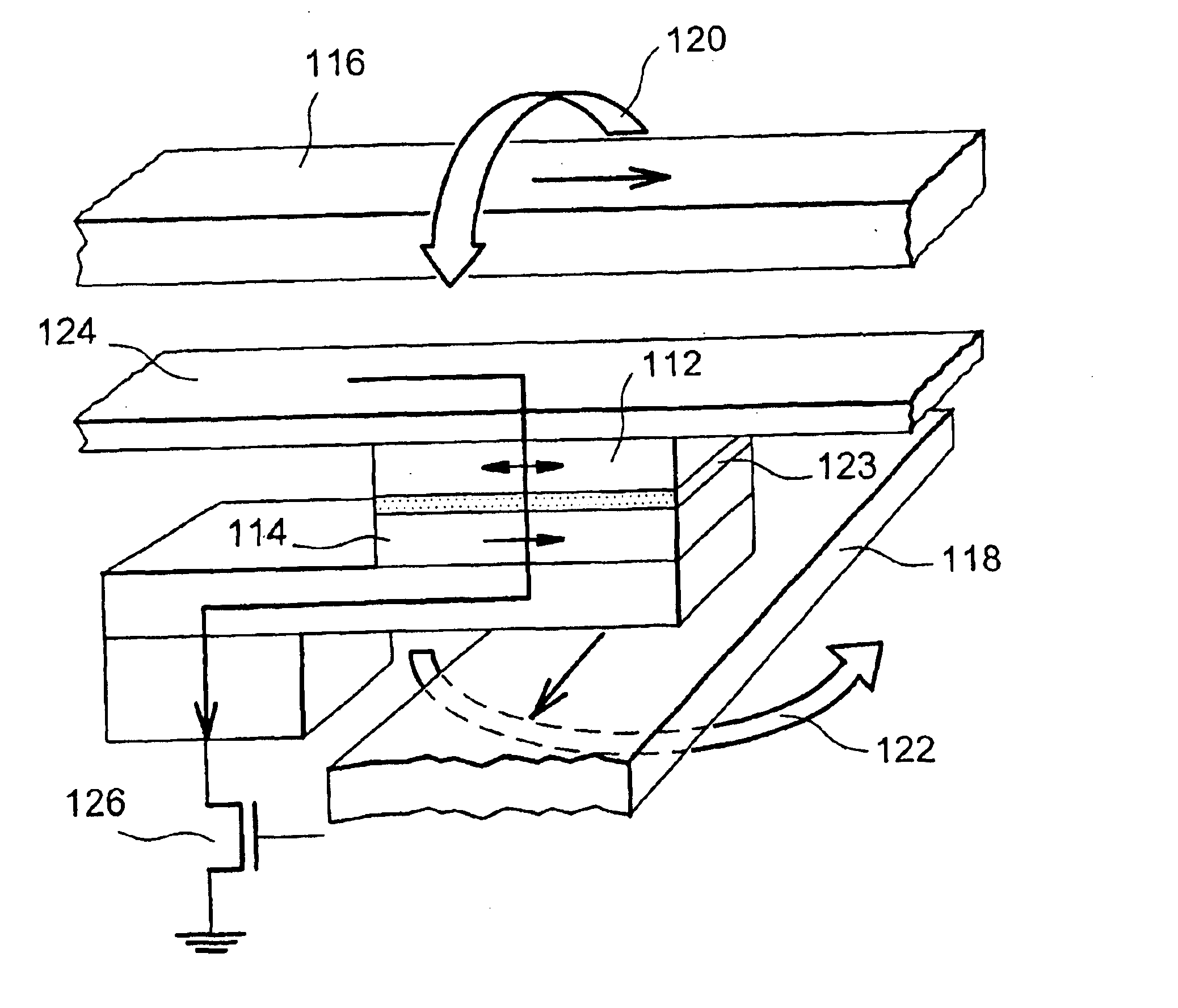
first embodiment
[0118]In the invention, the magnetisations of the two layers F1 and F2 are perpendicular to the plane of the layers or, more precisely, to the interfaces of said layers.
[0119]Layers F1 and F2 may comprise a pure material, an alloy or a series of alternating layers, certain of which are magnetic.
[0120]Co layers, of hexagonal structure, have their magnetisation perpendicular to the plane of these layers if the axis c of the hexagonal lattice is perpendicular to the plane of the sample containing said layers. Alloy layers such as CoPt, FePd and FePt may also have magnetisations perpendicular to their planes. Finally, multi-layers comprising alternating layers of two different materials at least one of which is magnetic, such as for example Co 0.6 nm / Pt 1.4 nm, may also have magnetisations perpendicular to the plane.
[0121]The cobalt may easily be replaced by an alloy rich in Co (greater than 70%) with for example Fe or Ni or Cr.
[0122]An example of forming a multi-layer Co / Pt based magne...
second embodiment
[0154]In the invention, the magnetisations of the two layers F1 and F2 are parallel to the plane of the layers or, more precisely, to the interfaces of said layers.
[0155]As previously, the magnetic materials making up the magnetic tunnel junction must be chosen in such a way that one has a faster thermal decrease of its coercive field than the other.
[0156]The material of the reference layer F2 may be an alloy based on Co, Fe, Ni (for example CO90Fe10) and its magnetisation may be pinned by an exchange interaction with an antiferromagnetic material with high blocking temperature (a lot higher than 200° C.) such as PtMn.
[0157]The material of layer F1 may be formed of an alloy in which the Curie temperature is reduced in volume to enable the switch over of its magnetisation to be facilitated when said material is heated to around 200° C.
[0158]An advantageous means of obtaining this property consists in coupling the magnetisation of the storage layer to an antiferromagnetic layer with l...
PUM
| Property | Measurement | Unit |
|---|---|---|
| temperature | aaaaa | aaaaa |
| temperature Tmax | aaaaa | aaaaa |
| magnetisation | aaaaa | aaaaa |
Abstract
Description
Claims
Application Information