System for the formation of a silicon thin film and a semiconductor-insulating film interface

a technology of semiconductor insulation film and silicon thin film, which is applied in the field of system for the formation of silicon thin film and semiconductor insulation film interface, can solve the problems that the connection pitch of the tab connection or the wire bonding method cannot be significantly reduced, the characteristics of the polycrystalline silicon thin film transistor cannot be satisfactorily uniform, etc., to achieve satisfactory semiconductor insulation film interface and reduce plasma damage

Inactive Publication Date: 2005-03-01
NEC CORP +1
View PDF51 Cites 155 Cited by
  • Summary
  • Abstract
  • Description
  • Claims
  • Application Information

AI Technical Summary

Benefits of technology

Accordingly, an object of the invention is to provide a process for forming a semiconductor thin film with a reduced trap state density by light irradiation and to provide a process and system for applying the above process to large substrates with a high reproducibility.
By the configuration where the plasma generating chamber is separated from the substrate process chamber, damage induced by plasma can be reduced to yield a satisfactory gate insulating film. In addition, the trap state density of the semiconductor thin film becomes equal to or less than the interface state density, and a satisfactory semiconductor-insulating film interface can be obtained.

Problems solved by technology

A conventional tab connection method or wire bonding method cannot significantly provide such a decreased connection pitch.
However, if a process at high temperatures as in the above case is employed in the polycrystalline silicon TFT process, low softening point glasses cannot be employed.
The resulting polycrystalline silicon thin film and polycrystalline silicon thin film transistor cannot therefore have satisfactorily uniform characteristics.
However, according to this process, a rather weak light is oscillated even though the formation of spiking is inhibited.
The resulting transistor element and thin film integrated circuit cannot have a significant uniformity in the substrate plane.
However, this technique cannot be applied to a process of intermittently repeating the lasing and the movement of stage.
However, although this process can stably irradiate the substrate with a laser beam, the process also yields increased excess lasing that does not serve to the formation of a polycrystalline silicon thin film.
The productivity is decreased from the viewpoint of the life of an expensive laser source and an excited gas, and the production efficiency of the polycrystalline silicon thin film is deteriorated with respect to power required for lasing.
The production costs are therefore increased.
When a substrate to be exposed to laser is irradiated with an excessively strong light as compared with a target intensity, the substrate will be damaged.
Such an excessively strong light is induced by an irregular irradiation intensity.
In LCDs and other imaging devices, a light passing through the substrate scatters in an area where the substrate is damaged, and the quality of image is deteriorated.
Accordingly, a crystalline silicon thin film having a desired uniformity cannot be significantly obtained.
In addition, as an ultraviolet radiation with a short wavelength is reduced and projected, the focal depth of the beam is small and the irradiation depth is liable to shift due to warp or deformation of the substrate.
With an increasing area of the substrate, the mechanical precision of the stage cannot be significantly ensured, and a little tilt of the stage or a displacement of the substrate on the stage disturbs a target laser irradiation.
However, as pointed out in the above reference, such an increased irradiation energy invites the resulting film to become amorphous or microcrystalline.
Particularly, when the cooling rate in cooling procedure is extremely large and the material undergoes an excessive supercooling, the material is not crystallized at around its solidification point, and becomes an amorphous solid due to quenching and rapid solidification.
Specifically, the surface of silicon formed by laser-induced crystallization is very active, and when the surface is exposed to the air, impurities are liable to adhere to the surface.
Specifically, to obtain satisfactorily advantages of a clean surface of a sample that is obtained by forming a silicon film and a gate insulating film in the same system without exposing the substrate to the air, the performance (the trap state density) of the silicon film is still insufficient.
However, this advantage is restricted by the performances of a silicon film which is previously formed.

Method used


Image

  • System for the formation of a silicon thin film and a semiconductor-insulating film interface
  • System for the formation of a silicon thin film and a semiconductor-insulating film interface
  • System for the formation of a silicon thin film and a semiconductor-insulating film interface

Examples


first embodiment

Next, the CVD system according to the invention will be illustrated with reference to FIGS. 36 and 37. In the CVD system shown in FIG. 36, a silicon oxide film as a gate insulating film is formed on a conventional TFT glass substrate 7111, using, preferably, silane as a material gas. A casing 7112 of the CVD system is a vacuum casing, and the inside of the casing is maintained at a desired degree of vacuum during film forming operation by action of an evacuating mechanism 7113. The evacuating mechanism 7113 is connected to an evacuating port 7112b-1 formed in the vacuum casing 7112.

The vacuum casing 7112 houses a partition 7114 at the midpoint in a vertical direction. The partition 7114 is composed of a conductive material and is arranged in a nearly horizontal position, and has, for example, a square plane shape. The periphery of the partition 7114 is in contact with a peripheral wall of the vacuum casing 7112. The partition 7114 serves to separate the inside of the vacuum casing 7...

second embodiment

this type of system will be described below. The system according to the second embodiment is characterized in that a laser annealing process and a gate insulating film forming process can be continuously performed in vacuo. These processes are required for the production of a TFT-LCD using a polysilicon film as a channel layer. In the system according to the second embodiment, the transfer chamber 8103 also includes the pressure regulating gas inlet system 8132, and the inside of the transfer chamber 8103 is held at a pressure that is a vacuum pressure but is higher than 1 Pa and lower than that in the film forming chamber 8101. The pressure regulating gas inlet system 8132 brings a hydrogen gas into the transfer chamber 8103 as mentioned above.

According to the second embodiment, the surface of the substrate 8109 is modified by supplying a modifier after the annealing process. This configuration plays a very important role to improve the operating characteristics of the resulting T...


PUM

PropertyMeasurementUnit
temperatureaaaaaaaaaa
temperaturesaaaaaaaaaa
sizeaaaaaaaaaa

Abstract

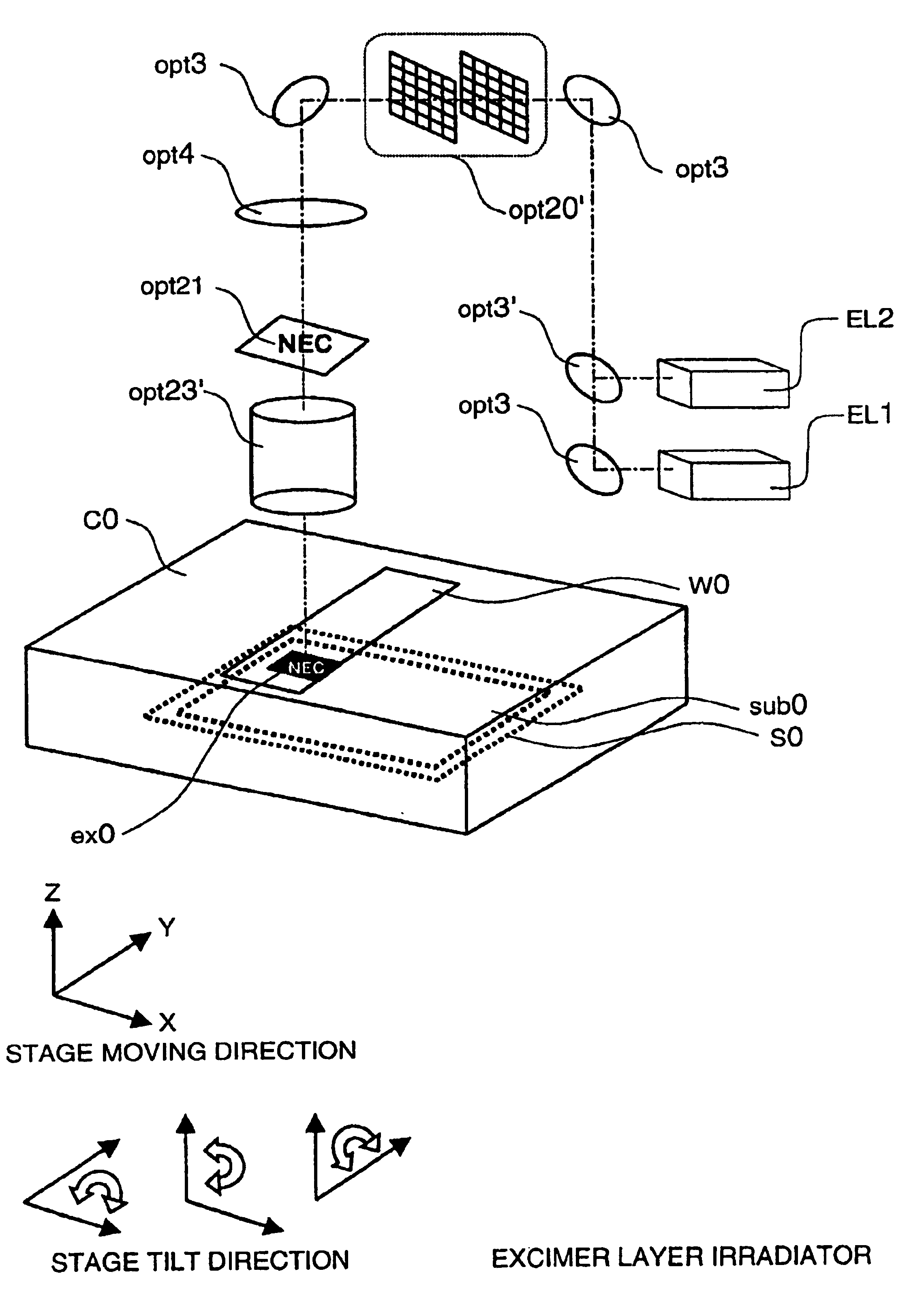
In a semiconductor thin film forming system for modifying a predetermined region of a semiconductor thin film by exposing the semiconductor thin film to a projected light patterned through a pattern formed on a photo mask, the system includes a mechanism (opt20′) for uniformizing the light for exposure in a predetermined area on the photo mask. This system can provide a crystallized silicon film having a trap state density less than 1012 cm−2 and can provide a silicon-insulating film interface exhibiting a low interface state density.

Description

BACKGROUND OF THE INVENTION1. Field of the InventionThis invention relates to a system for the formation of a silicon thin film and a good-quality semiconductor-insulating film interface. Such silicon thin films are used for crystalline silicon thin film transistors, and such semiconductor-insulating film interfaces are employed for field effect transistors. The invention also relates to a semiconductor thin film forming system by the pulsed laser exposure method. Such semiconductors include, for example, silicon germanium (SiGe), silicon carbide (SiC), and other silicon compounds, and GaAs, GaN, CuInSe2, ZeSe, and other compound semiconductors. In addition, the invention relates to a system for the manufacture of driving elements or driving circuits composed of the semiconductor thin films or field effect thin film transistors for displays and sensors, for example.2. Description of the Related ArtTypical processes for the formation of a thin film transistor (TFT) on a glass substra...

Claims


Application Information

Patent Timeline
Patent Type & Authority Patents(United States)
IPC IPC(8): B23K26/067B23K26/06H01L21/02H01L21/20H01L21/205B23K26/073C23C14/28H01L21/027H01L21/268H01L21/336H01L29/786H01S3/00
CPCB23K26/04B23K26/046B23K26/0604B23K26/0608B23K26/063B23K26/0656B23K26/0732H01L21/2026H01L21/268H01L21/67225B23K26/043B23K26/067H01L27/1285B23K26/0622B23K26/066H01L21/0262H01L21/02683H01L21/02686H01L21/02422H01L21/02488H01L21/02678H01L21/02598H01L21/02532H01L21/0242H01L21/02691H01L21/027H01L21/02675
Inventor TANABE, HIROSHIAKASHI, TOMOYUKIWATABE, YOSHIMI
Owner NEC CORP
Why Eureka
Try Eureka