Voltage reference source adopting technique deviation compensation structure

A technology of voltage reference source and process deviation, applied in the direction of adjusting electrical variables, control/regulating systems, instruments, etc., can solve problems such as characteristic deviation of pnp transistors, and achieve the effect of high initial precision

Inactive Publication Date: 2009-12-30
XI AN JIAOTONG UNIV
View PDF2 Cites 0 Cited by
  • Summary
  • Abstract
  • Description
  • Claims
  • Application Information

AI Technical Summary

Problems solved by technology

[0022] 2) Deviation of pnp transistor characteristics

Method used


Image

  • Voltage reference source adopting technique deviation compensation structure
  • Voltage reference source adopting technique deviation compensation structure
  • Voltage reference source adopting technique deviation compensation structure

Examples


Embodiment Construction

[0043] The present invention will be described in further detail below in conjunction with the accompanying drawings.

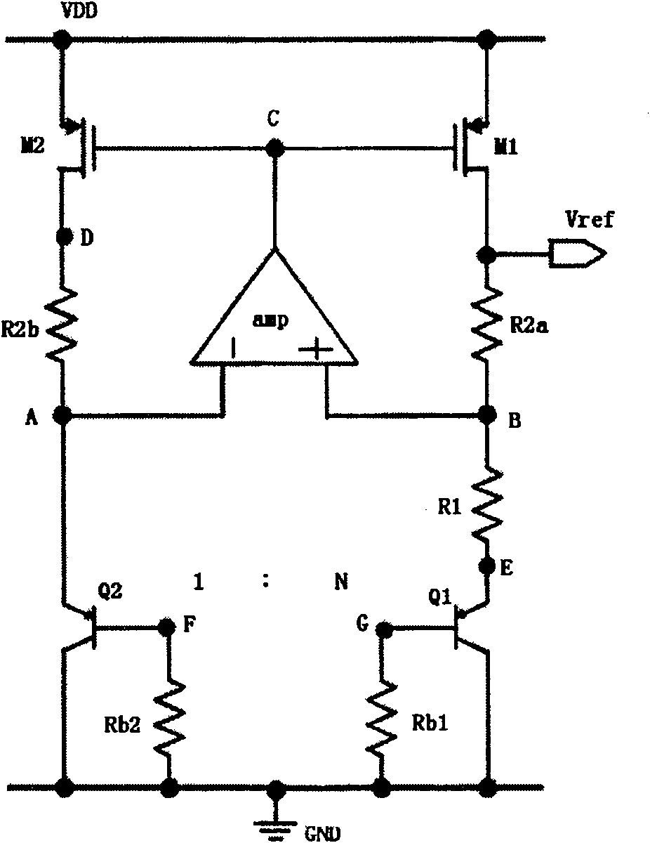
[0044] see figure 1 , the present invention includes MOS transistors M1 and M2, the source of MOS transistor M1 is connected to node VDD, the gate is connected to node C, the drain is connected to node Vref, the source of MOS transistor M2 is connected to node VDD, and the gate is connected to Node C, drain connected to node D, proportional resistor R 2a Connected between node B and node Vref, matching resistor R 2b Connected between node A and node D, the positive input of the error amplifier amp is connected to node B, the negative input is connected to node A, the output is connected to node C, and the transistor base-emitter dropout resistor R 1 Connected between node B and node E, the emitter of transistor Q1 is connected to node E, the base is connected to node G, and the collector is connected to node GND; the emitter of transistor Q2 is connected to...


PUM


Abstract

A voltage reference source adopts a process deviation compensating structure, wherein a process deviation compensating resistance is connected with the base electrode of a transistor, which ensures that the sum of the base electrode-emitter electrode voltage of the transistor and the voltage of the process deviation compensating resistance Rb1 can not be influenced by process deviation; therefore, the high precision voltage reference source, which has high initial precision and does not need correction, can be obtained.

Description

technical field [0001] The invention relates to a voltage reference source widely used in power supply chips, in particular to a voltage reference source adopting a process deviation compensation structure in a mixed signal chip. Background technique [0002] High-precision, low-cost voltage reference module is an important part of analog circuits and digital-analog hybrid circuits. At present, high-precision voltage reference sources are mainly manufactured using bipolar technology and BiCMOS technology, and after the chip is completed, special correction technology is required to ensure its accuracy. However, these processes are complicated in technology, high in manufacturing cost, and incompatible with mainstream CMOS processes, and corrections to chips one by one will greatly reduce production efficiency. [0003] The current CMOS integrated circuits occupy about 90% of the market. Highly integrated products and mixed integration of digital and analog circuits have bec...

Claims


Application Information

Patent Timeline
Patent Type & Authority Patents(China)
IPC IPC(8): G05F3/24
Inventor 邵志标傅懿斌
Owner XI AN JIAOTONG UNIV
Why Eureka
Try Eureka