Thin layer transfer method wherein a co-implantation step is performed according to conditions avoiding blisters formation and limiting roughness

A thin-layer, conditional technology, applied in the field of thin-layer structure of semiconductor materials, can solve the problems of inability to separately control surface roughness and bubble formation, undesirable bubble formation, poor roughness, etc.

Active Publication Date: 2007-08-29
SOITEC SA
View PDF0 Cites 2 Cited by
  • Summary
  • Abstract
  • Description
  • Claims
  • Application Information

AI Technical Summary

Problems solved by technology

[0043] Therefore, as is clearly seen from the comparison of Tables 1 and 2, certain injection conditions that lead to the best roughness lead to undesired bubble formation, and conversely, conditions that avoid bubble formation lead to poor roughness
[0044] From this it appears that surface roughness and bubble formation cannot be controlled separately

Method used


Image

  • Thin layer transfer method wherein a co-implantation step is performed according to conditions avoiding blisters formation and limiting roughness
  • Thin layer transfer method wherein a co-implantation step is performed according to conditions avoiding blisters formation and limiting roughness
  • Thin layer transfer method wherein a co-implantation step is performed according to conditions avoiding blisters formation and limiting roughness

Examples


Embodiment Construction

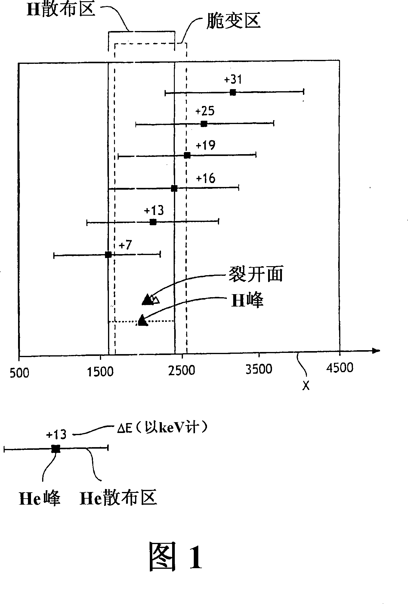
[0067] As already revealed, the present invention relates to a co-implantation step performed during the fabrication of a structure comprising a thin layer of semiconductor material on a support substrate through the level of the donor substrate previously embrittled by the implantation of the species obtained separately.

[0068] The present invention can help to improve the quality of structures obtained by using SMARTCUT-type transfer processes.

[0069] In general, the structure may be any type of structure comprising a thin layer of semiconducting material on a surface exposed to the external environment.

[0070] In a non-limiting manner, the thin layer of semiconductor material may be silicon Si, silicon carbide SiC, germanium Ge, silicon-germanium SiGe, gallium arsenide AsGa, or the like.

[0071] The substrate support can be made of silicon Si, quartz or the like.

[0072] It is also possible to insert a layer of oxide between the supporting substrate and the thin l...


PUM


Abstract

The present invention proposes a method of transferring thin layers in which two different kinds of co-implantation steps are performed. The implant energies of the first and second species are selected such that the second species peak is located in the thickness of the donor substrate within the embrittlement region and deeper than the first species dispersion region, and the first species is selected The implant dose of the second type is substantially similar, and the implant dose of the first type accounts for 40% to 60% of the total implant dose.

Description

technical field [0001] The invention relates to a method for manufacturing a structure comprising a thin layer of semiconductor material on a substrate, comprising the steps of: [0002] perform a species implant under the face of the donor substrate where a thin layer has to be made to create an embrittlement zone in the thickness of the donor substrate, [0003] after implantation, bringing the face of the donor substrate into intimate contact with the support substrate, [0004] • Detaching the donor substrate at the level of the embrittlement zone to transfer a portion of the donor substrate onto the support substrate and form a thin layer on the support substrate. [0005] The present invention relates more precisely to the injection step mentioned above. Background technique [0006] A SMARTCUT-type process, which is an example of a method of the type mentioned above and corresponds to a preferred embodiment of the present invention, more full details of which can be...

Claims


Application Information

Patent Timeline
Patent Type & Authority Applications(China)
IPC IPC(8): H01L21/762
CPCH01L21/76254H01L21/26506
Inventor N·P·阮N·本穆罕默德A·布萨戈尔T·赤津G·苏丘
Owner SOITEC SA
Why Eureka
Try Eureka