Ion implantation high temperature target

A technology of ion implantation and target disk, which is used in the manufacture of discharge tubes, electrical components, semiconductor/solid state devices, etc.

Inactive Publication Date: 2007-09-19
48TH RES INST OF CHINA ELECTRONICS TECH GROUP CORP
View PDF0 Cites 4 Cited by
  • Summary
  • Abstract
  • Description
  • Claims
  • Application Information

AI Technical Summary

Problems solved by technology

However, the existing high-temperature target disk

Method used


Image

  • Ion implantation high temperature target
  • Ion implantation high temperature target
  • Ion implantation high temperature target

Examples


Example Embodiment

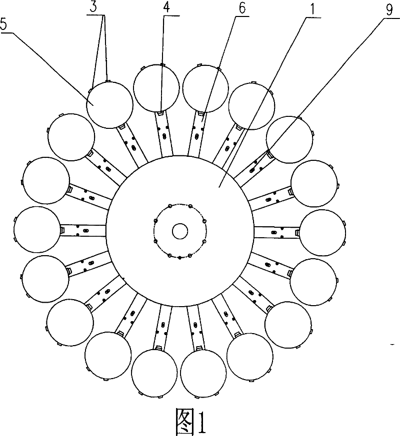
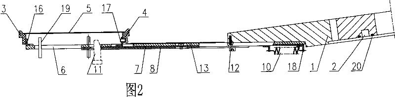
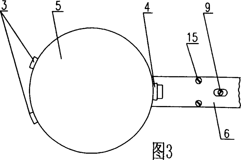
[0031]Refer to the attached drawings. The target base 1 is made of aluminum with good thermal conductivity. Its cooling water path is an annular water tank 2, and it can also be a water jacket composed of two sealing rings 20. The interior is cooled by water and is in a low temperature area. ; The wafer clamping mechanism in the high temperature zone is connected to the target base 1 through the support bar 6 in the temperature transition zone, and the motor drives the target base 1 to rotate. The whole target is designed to hold 18 wafers, and the target claw group clamps the wafer for work Uniform speed rotation (to ensure the high temperature requirements of the wafer during injection, make full use of the heat source and improve thermal efficiency, the structural size of the parts in this area should be as small as possible, designed with the smallest quality and the smallest heat conduction area; to ensure that the wafer is injected at high temperature The surface temperature...


PUM


Abstract

The invention provides an ion implantation high temperature target which includes a target pedestal with cooling groove, and wafer clamping mechanism disposed at the periphery of the target pedestal and connected to the same by a support bar, a two-point clip fixed to the outer end of the support bar by a connection angle-block, a concave groove arranged on the support bar and in which a movable plate is disposed, the concave surface of the support bar, which has a silicon liner plate, provided with a cover plate, a single-point clip fixed to the front part of the movable plate, the two ends of the clamping spring at the inner end of the support bar respectively connected to support bar and the movable plate and moving the movable plate toward the center of the wafer by the force of the clamping spring; the movable plate is provided with limit nail, and the support bar is provided with a wafer support pillar having an inclined top face and disposed at the outer end of the movable plate, and a wafer support rod which can move up and down; the two-point clip and the single-point clip are made of high purity silica, and the support bar, the movable plate, the cover plate, the each connection angle block, the bolt are made of molybdenum material. The invention enables the high temperature ion implantation machine to continuously and normally implant the semiconductor wafer in high temperature condition of 400 to 800 DEG C..

Description

technical field [0001] The invention relates to semiconductor material production equipment, in particular to an ion implantation high-temperature target disk used for an ion implanter. Background technique [0002] In the field of semiconductor IC manufacturing, the development of ultra-large-scale integrated circuits poses new and severe challenges to further improve the integration level and operating speed of chips, reduce the feature size of integrated circuits, and enhance radiation resistance. SOI technology is the solution VLSI power consumption crisis and the key technology to improve radiation resistance, it will gradually replace bulk silicon as the mainstream technology of deep submicron integrated circuits, and it is also the preferred technology for processes below 0.13μm. SOI materials are also used in aerospace and other weapons and equipment It is an essential material for fierce competition in the field and will be the leading material for VLSI in the futur...

Claims


Application Information

Patent Timeline
IPC IPC(8): H01J37/317H01J37/02H01L21/265H01L21/425
Inventor 贾京英刘咸成王慧勇
Owner 48TH RES INST OF CHINA ELECTRONICS TECH GROUP CORP
Why Eureka
Try Eureka