
Light-emitting element, manufacturing method thereof, light-emitting device, and electronic device

A technology of light-emitting components and manufacturing methods, which is applied in the direction of electroluminescent light sources, electrical components, luminescent materials, etc., and can solve problems such as difficulty in obtaining light

Inactive Publication Date: 2007-12-05
SEMICON ENERGY LAB CO LTD
View PDF2 Cites 0 Cited by
  • Summary
  • Abstract
  • Description
  • Claims
  • Application Information

AI Technical Summary

Problems solved by technology

However, when the luminescent material produced by these methods is used in a thin-film inorganic EL element, there is a problem that it is difficult to obtain luminescence having a plurality of luminescence wavelength peaks.

Method used


Image

  • Light-emitting element, manufacturing method thereof, light-emitting device, and electronic device
  • Light-emitting element, manufacturing method thereof, light-emitting device, and electronic device
  • Light-emitting element, manufacturing method thereof, light-emitting device, and electronic device

Examples


Embodiment approach 1

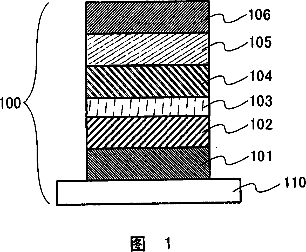
[0145] In this embodiment mode, a method for manufacturing a thin-film light-emitting element of the present invention will be described with reference to FIG. 1 .

[0146] 1 is a thin film element 100, which has on a substrate 110: a first electrode 101 and a second electrode 106; a first insulating layer 102 and a second insulating layer 105 adjacent to each electrode; The light-emitting layer formed by the first layer 103 and the second layer 104 is between the two insulating layers 105 . This embodiment mode is a method of manufacturing a light-emitting element capable of obtaining light emission from a light-emitting layer by performing heat treatment after forming a thin film, and will be described below.

[0147] The substrate 110 serves as a support for the light emitting element. As the substrate, for example, glass, quartz, or plastic can be used. In addition, as long as it can function as a support body in the process of manufacturing a light-emitting element, the...

Embodiment approach 2

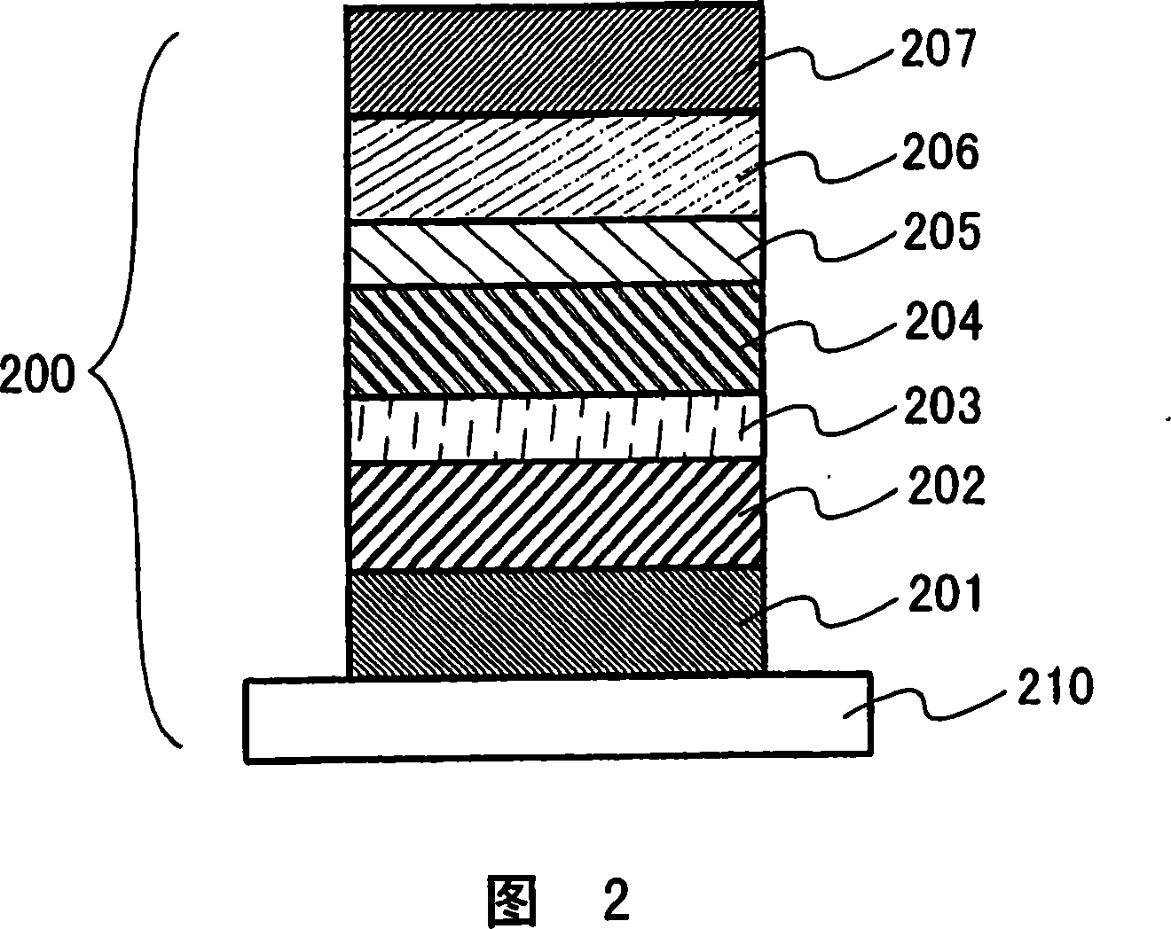
[0157] In this embodiment mode, a thin film light emitting element of the present invention will be described with reference to FIG. 2 .

[0158] 2 is a thin film element 200, which has on a substrate 210: a first electrode 201 and a second electrode 207; a first insulating layer 202 and a second insulating layer 206 adjacent to each electrode; The light-emitting layer composed of the first layer 203 , the second layer 204 and the third layer 205 is between the two insulating layers 206 . As in Embodiment 1, a light-emitting element capable of emitting light from a light-emitting layer obtained by performing a heat treatment after forming a thin film will be described below.

[0159] The materials described in Embodiment 1 can be used for the substrate 210 , the first electrode 201 and the second electrode 207 , and the first insulating layer 202 and the second insulating layer 206 .

[0160] The first layer 203 and the third layer 205 are layers containing a luminescent cent...

Embodiment approach 3

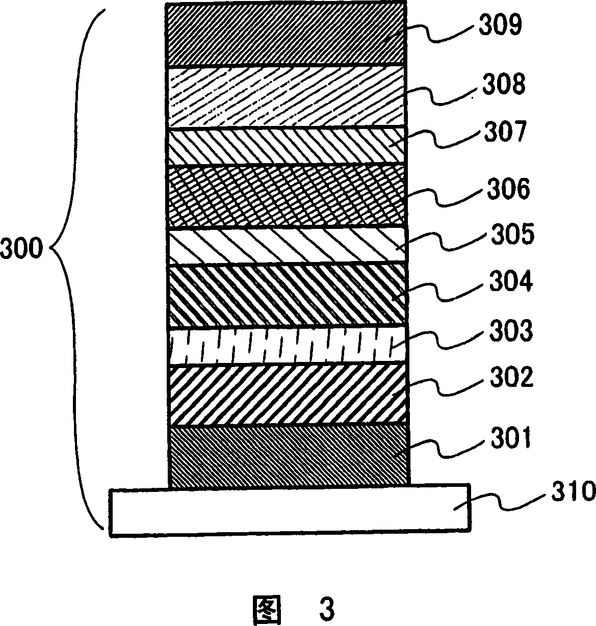
[0166] In this embodiment mode, a thin film light emitting element of the present invention will be described with reference to FIG. 3 .

[0167] 3 is a thin film element 300, which has on a substrate 310: a first electrode 301 and a second electrode 309; a first insulating layer 302 and a second insulating layer 308 adjacent to each electrode; The first layer 303 , the second layer 304 , the third layer 305 , the fourth layer 306 and the fifth layer 307 between the two insulating layers 308 . As in Embodiment 1, by performing heat treatment after forming a thin film, light emission can be obtained from a plurality of layers containing a matrix material constituting a light emitting layer, as will be described below.

[0168] The materials described in Embodiment 1 can be used for the substrate 310 , the first electrode 301 and the second electrode 309 , and the first insulating layer 302 and the second insulating layer 308 .

[0169] The first layer 303, the third layer 305,...


PUM


Abstract

It is an object of the present invention to provide a manufacturing method for a light-emitting element that emits light at a plurality of emission wavelength peaks. Furthermore, it is an object of the present invention to provide a light-emitting device and electronic device in which color rendering is high. A manufacturing method for a light-emitting element includes the following steps: a step for forming a first electrode, a step for forming a light-emitting layer over the first electrode, a step for forming a second electrode over the light-emitting layer, and a step for performing heat treatment on the light-emitting layer; where the step for forming the light-emitting layer includes a step for forming a layer containing a host material and a layer containing a material acting as a luminescent center so that the two layers are in contact with each other.

Description

technical field [0001] The present invention relates to a light-emitting element utilizing electroluminescence. Furthermore, the present invention relates to a light-emitting device and electronic equipment including a light-emitting element. Background technique [0002] In recent years, display devices such as televisions, mobile phones, and digital cameras have been required to be thin flat display devices, and display devices using self-luminous light-emitting elements have attracted attention as display devices meeting this requirement. As one of the self-luminous light-emitting elements, there is a light-emitting element utilizing electroluminescence (Electro Luminescence), and by applying a voltage to a light-emitting element in which the light-emitting material is sandwiched between a pair of electrodes, light emission can be obtained from the light-emitting material. [0003] Such self-luminous light-emitting elements have advantages over liquid crystal displays, s...

Claims


Application Information

Patent Timeline
Patent Type & Authority Applications(China)
IPC IPC(8): H01L33/00H05B33/14H05B33/10
CPCH05B33/14C09K11/574C09K11/612H05B33/20
Inventor 坂田淳一郎
Owner SEMICON ENERGY LAB CO LTD
Learn More