Manufacturing method of circuit board encapsulated by accumulation circuit

A circuit board manufacturing and integrated circuit technology, which is applied in chemical/electrolytic methods to remove conductive materials, printed circuit components, and secondary processing of printed circuits, etc. higher question

Inactive Publication Date: 2007-12-12
LONGQUAN INT
View PDF0 Cites 2 Cited by
  • Summary
  • Abstract
  • Description
  • Claims
  • Application Information

AI Technical Summary

Problems solved by technology

[0020] The positive film process steps include chemical through-holes, circuit fabrication, circuit etching and circuit surface treatment: However, since the circuit etching will form two copper surfaces with different surface areas, it is easy to form a coating after the (COB) surface coating process. Uneven thickness, and in the molding and sealing process of integrated circuit packaging (COB), it is easy to cause mold overflow due to unevenness; moreover, only a part of the required circuit is left,

Method used


Image

  • Manufacturing method of circuit board encapsulated by accumulation circuit
  • Manufacturing method of circuit board encapsulated by accumulation circuit
  • Manufacturing method of circuit board encapsulated by accumulation circuit

Examples


Embodiment Construction

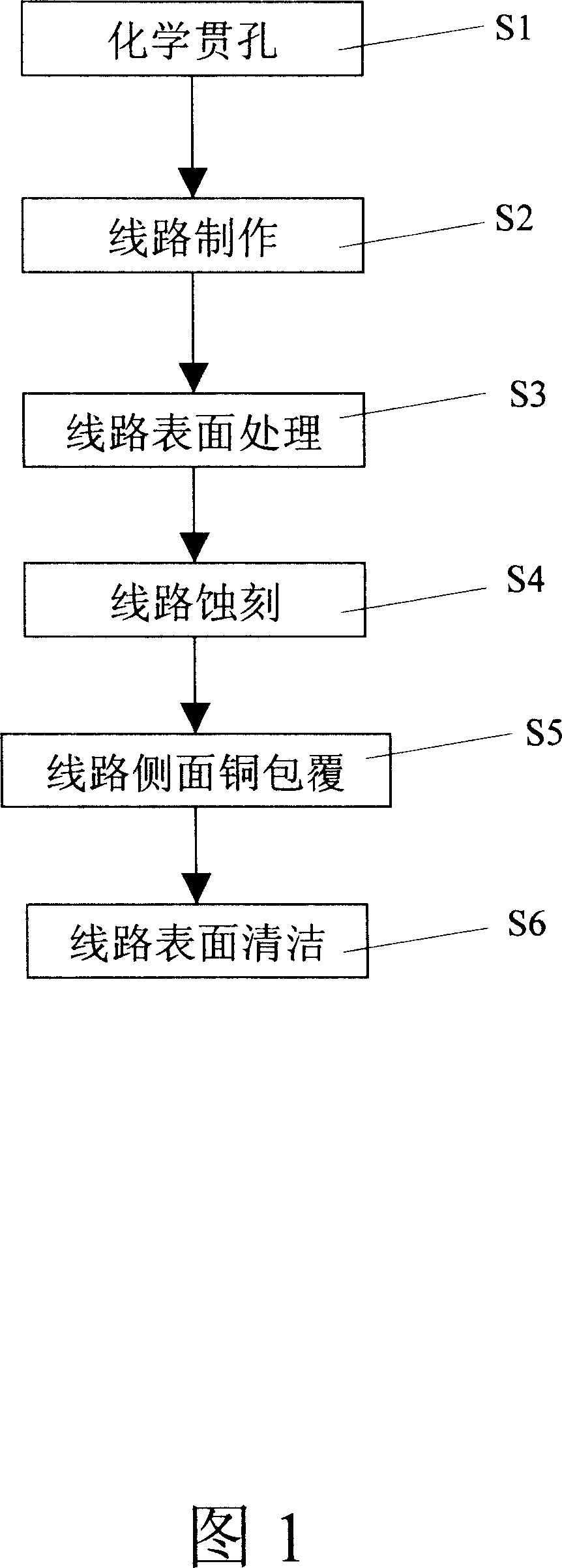
[0042] The invention provides a circuit board manufacturing method applied to integrated circuit packaging.

[0043] First, please refer to Figure 1, the steps include:

[0044] Step 1 (S1), chemical through hole: make a chemical through hole (PTH) on the copper circuit board to make the upper and lower copper surfaces conductive;

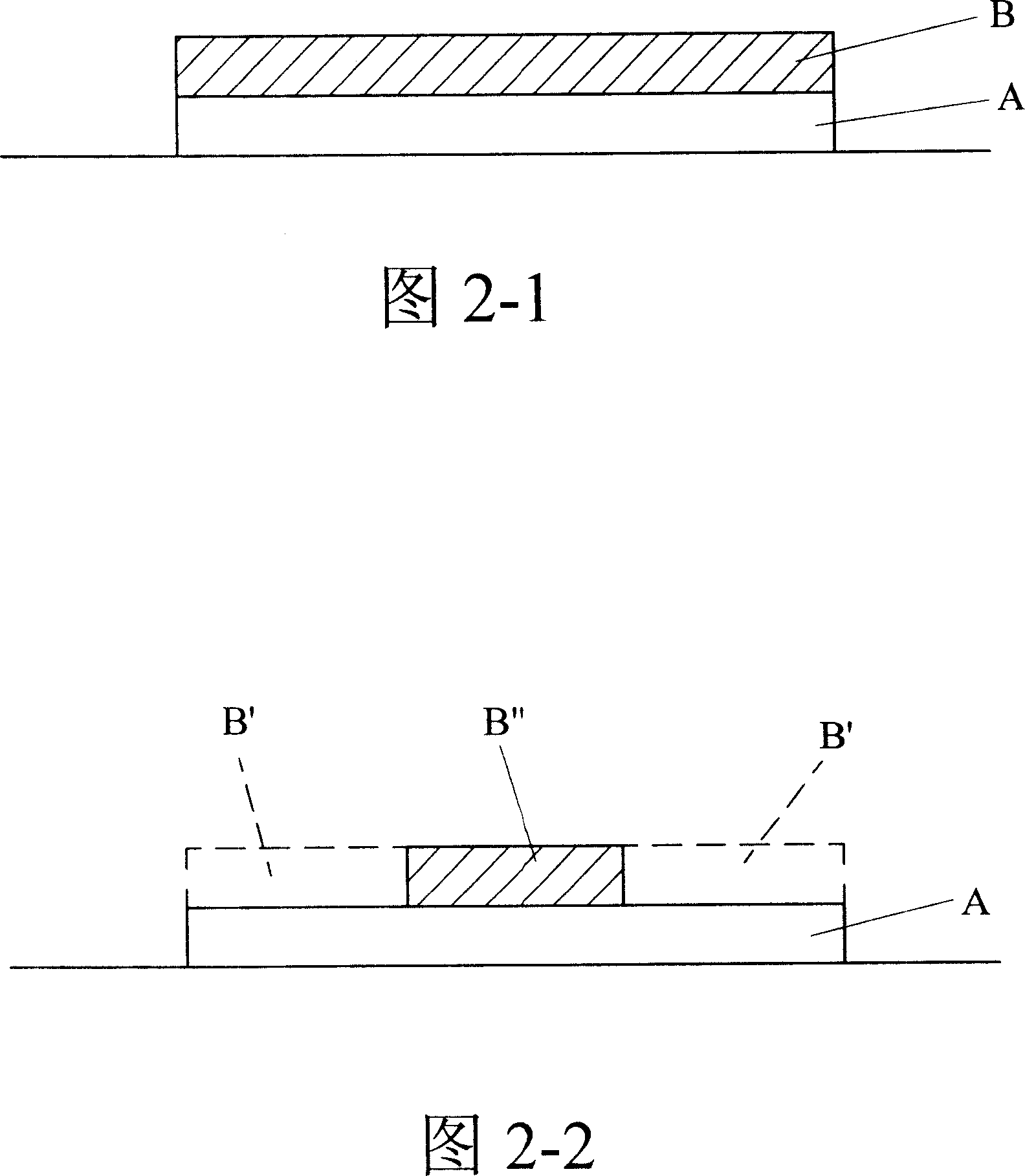
[0045] Step 2 (S2), circuit production: use liquid ink or photosensitive ink to form a circuit through the film and light source exposure principle (as shown in Figure 2-1, the copper layer is A, and the ink is B), and then remove it chemically Ink on the surface of the circuit to expose the copper layer on the surface of the circuit (as shown in Figure 2-2, the removed ink is B', the remaining ink B", and the underlying copper layer A can be exposed after ink B' is removed) .

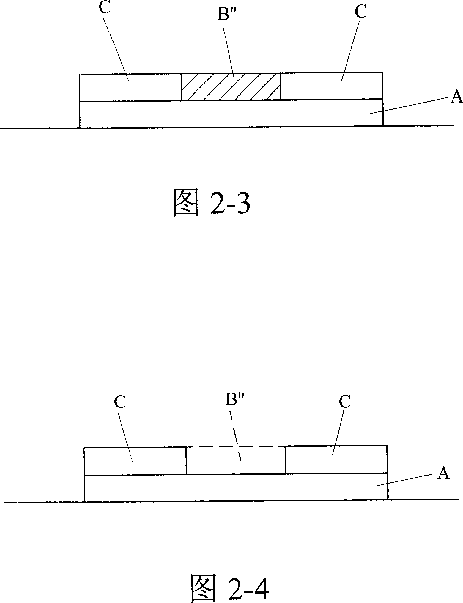
[0046] Step 3 (S3), circuit surface treatment: after removing the remaining ink on the circuit surface, the exposed copper surface is plated with a metal layer conforming...


PUM


Abstract

A kind of circuit board producing method which is applied to circuit enclosing, before the printed circuit board is etched, the surface of line is processed, metal layer which fulfills circuit board producing (COB) is plated; high-low current effect generated by area when wiring can be avoided, and phenomenon that difference of metal layer of circuit board producing (COB) is too big can be avoided; beside, surface of circuit board producing (COB) does not need wire, so area of wiring during design can be increased.

Description

technical field [0001] The invention provides a circuit board manufacturing method applied to integrated circuit packaging, especially an integrated circuit packaging process that can reduce costs. technical background [0002] Manufacturing methods of traditional printed circuit boards, including positive film process and negative film process; [0003] The manufacturing process of the traditional positive film is shown in Figure 3, and its steps include: [0004] X1: chemical through hole: make a chemical through hole (PTH) on the copper circuit board to make the upper and lower copper surfaces conductive; [0005] X2: Circuit production: use liquid ink or photosensitive ink to form circuits through the film and light source exposure principle, and then chemically remove the non-circuit surface ink to expose the copper layer on the surface; [0006] X3: Circuit etching: use the principle of chemical corrosion to decompose the exposed copper layer to completely remove the...

Claims


Application Information

Patent Timeline
IPC IPC(8): H05K3/06H05K3/22H05K1/09
Inventor 黄进发简惠玲
Owner LONGQUAN INT
Why Eureka
Try Eureka