Supercharge Your Innovation With Domain-Expert AI Agents!

Band-gap reference circuit

A reference circuit and band difference technology, applied in the direction of adjusting electrical variables, control/regulating systems, instruments, etc., can solve problems such as the inability to provide reference voltages, the inability of semiconductor process band difference reference circuits to provide accurate reference voltages, and semiconductor process errors.

Inactive Publication Date: 2008-01-16
FARADAY TECH CORP
View PDF0 Cites 6 Cited by
  • Summary
  • Abstract
  • Description
  • Claims
  • Application Information

AI Technical Summary

Problems solved by technology

[0027] Due to the offset of the semiconductor process, the reference voltage (Vref) provided by the band difference reference circuit will produce an error of about ±15%, resulting in the band difference reference circuit of Figure 4 being unable to provide an accurate reference voltage (Vref).
Therefore, how to improve the offset of the known semiconductor process and cause the problem that the band difference reference circuit cannot provide an accurate reference voltage (Vref) is the main purpose of the present invention

Method used


Image

  • Band-gap reference circuit
  • Band-gap reference circuit
  • Band-gap reference circuit

Examples


Embodiment Construction

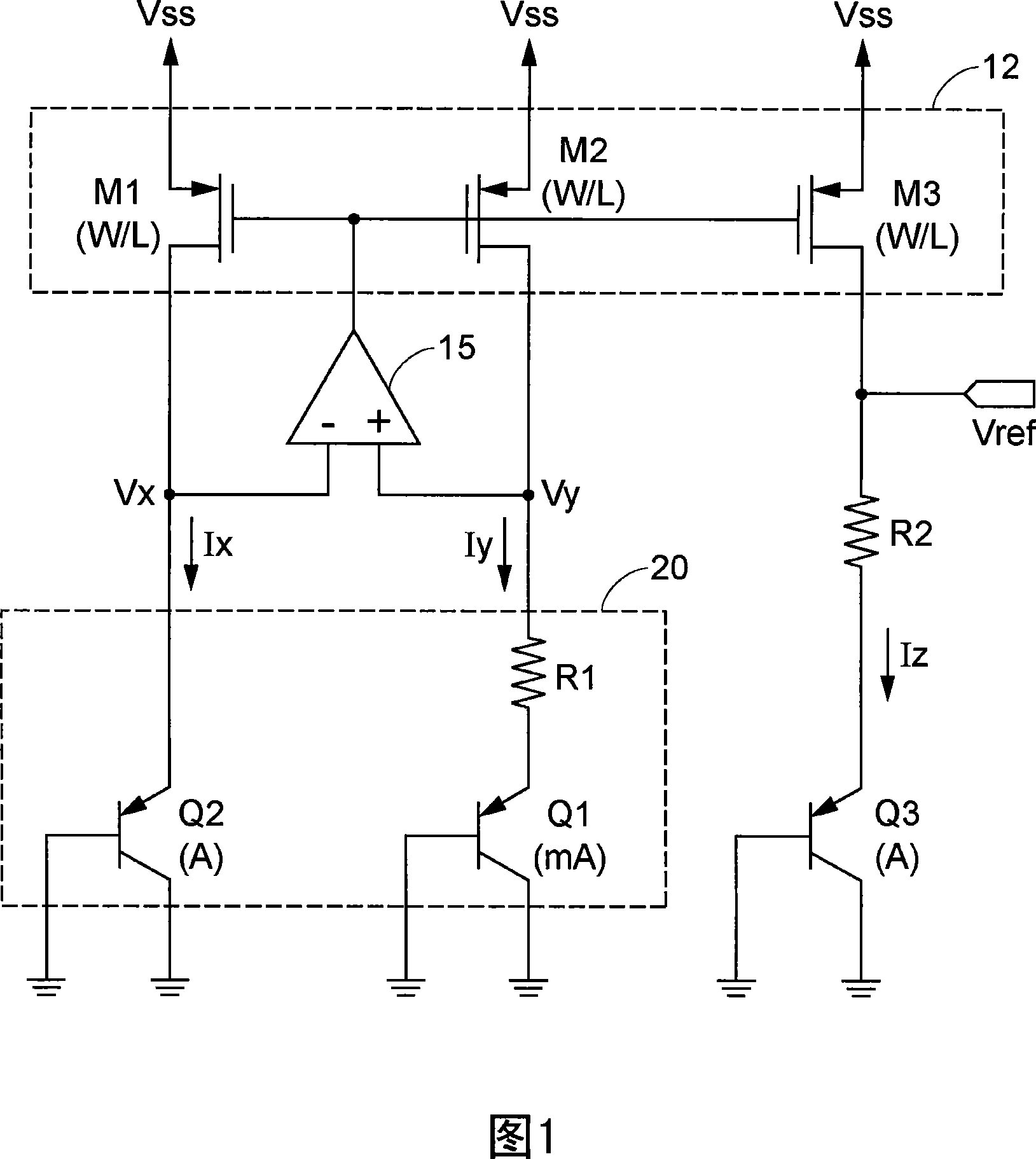
[0058] Please refer to FIG. 6 , which is a schematic diagram of the band difference reference circuit of the present invention. The band difference reference circuit includes a mirror circuit 142 , an operational amplifier 145 , and an input circuit 150 . The mirror circuit 142 includes three PMOS field effect transistors M1 , M2 , M3 , and in this example, M1 , M2 , M3 have the same aspect ratio (W / L). The gates of M1, M2 and M3 are connected to each other, the sources of M1, M2 and M3 are connected to the power supply (Vss), and the drains of M1, M2 and M3 can respectively output currents of Ix, Iy and Iz. In addition, the output of the operational amplifier 145 can be connected to the gates of M1, M2 and M3, the negative input of the operational amplifier 145 can be connected to the drain of M1, and the positive input of the operational amplifier 145 can be connected to the drain of M2. Furthermore, the input circuit 150 includes two NMOS field effect transistors M4, M5; w...


PUM


Abstract

The invention discloses a belt difference reference circuit which comprises an input circuit with two end points, a mirror image circuit which can control two output currents of two end points and maintains the invariable current proportion between the two output currents and a calculation amplifier which is connected with the two end points and the mirror image circuit to control the mirror image circuit so that the voltage between the two end points has voltage relation; wherein a first end point is connected with a first field effect transistor with a first critical voltage; a first resistance is connected between a second end point and a second field effect transistor with a second critical voltage; the first field effect transistor and the second field effect transistor are both operated in sub critical area; the first critical voltage is huger than the second critical voltage; the two output currents don't vary with the variable temperature.

Description

technical field [0001] The present invention relates to a bandgap reference circuit, and in particular to a low operating voltage bandgap reference circuit. Background technique [0002] As we all know, the function of the band difference reference circuit is to provide a stable reference voltage (Vref) that does not change with the process, temperature, and power supply voltage. Therefore, it is widely designed in many circuits in the field of hybrid circuits. For example, a voltage regulator (Voltage Regulator), a digital-to-analog circuit, and a low-drift amplifier (Low Drift Amplifier). [0003] Please refer to FIG. 1 , which is a schematic diagram of a known band difference reference circuit composed of a PMOS field effect transistor, a PNP bipolar transistor, and an operational amplifier. In general, the band difference reference circuit includes a mirroring circuit (Mirroring Circuit) 12 , an operational amplifier (Operation Amplifier) ​​15 , and an input circuit 20 ...

Claims


Application Information

Patent Timeline
Patent Type & Authority Applications(China)
IPC IPC(8): G05F3/16
Inventor 彭彦华王为善张家玮
Owner FARADAY TECH CORP
Features
  • R&D
  • Intellectual Property
  • Life Sciences
  • Materials
  • Tech Scout
  • Unparalleled Data Quality
  • Higher Quality Content
  • 60% Fewer Hallucinations
Learn More