Polishing pad
A polishing pad and annular groove technology, applied in the field of polishing pads, can solve the problems of complex polishing pad manufacturing, polishing pad peeling, and difficulty in distinguishing front and back sides from each other.
- Summary
- Abstract
- Description
- Claims
- Application Information
AI Technical Summary
Problems solved by technology
Method used
Image

Examples
Embodiment B
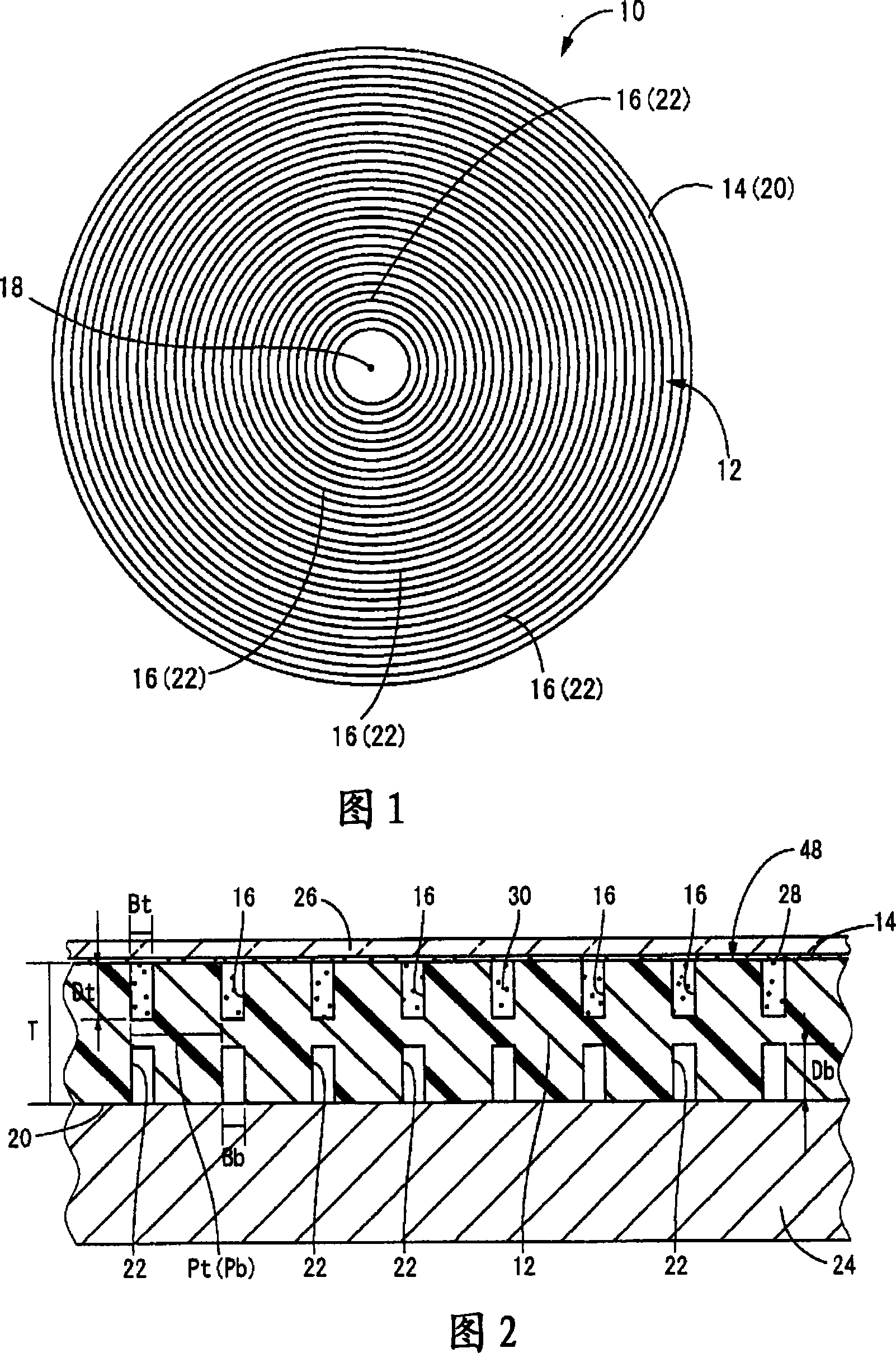
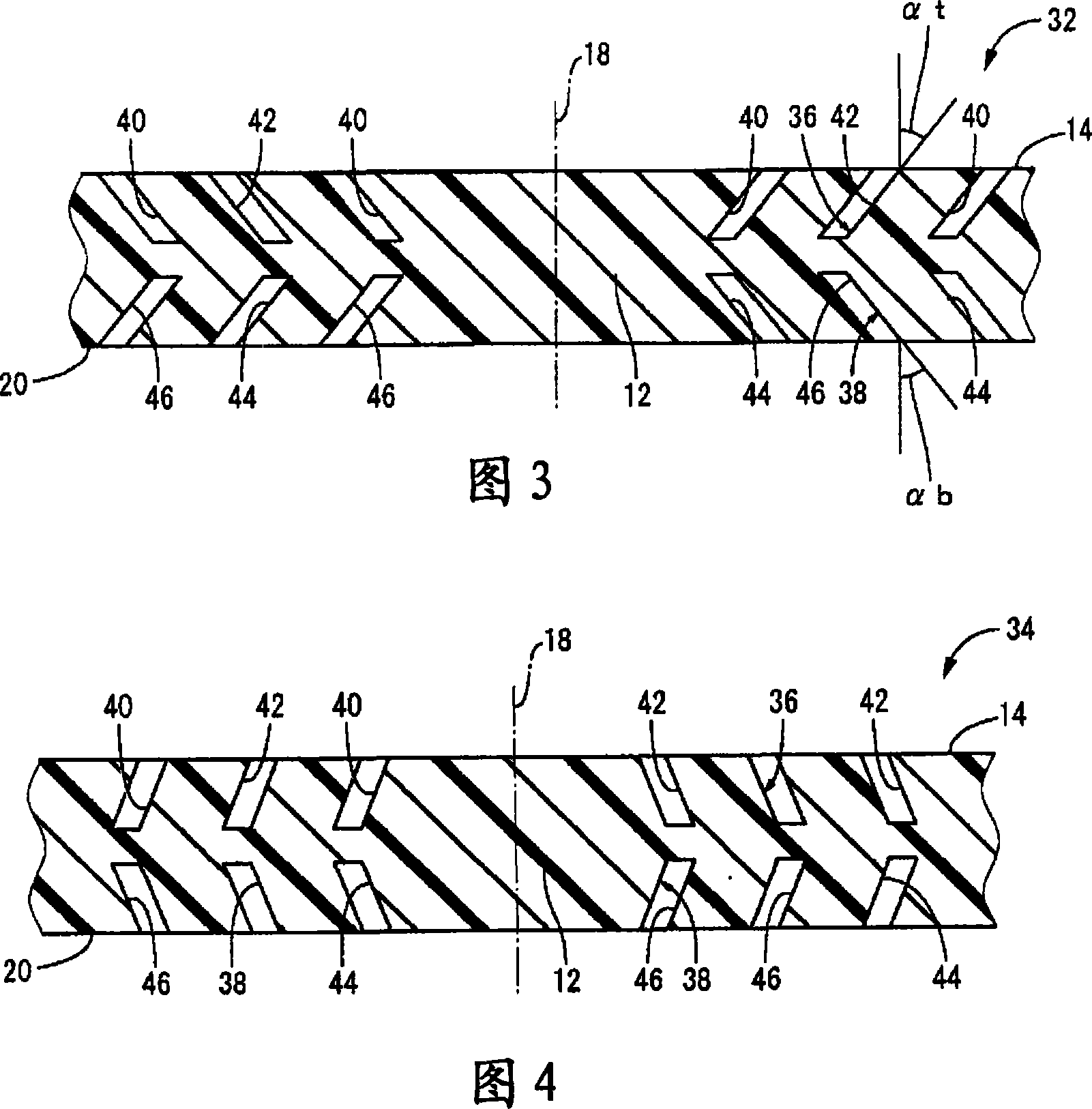
[0188] Referring to FIGS. 5-7 , there is shown a polishing pad 48 constructed in accordance with one embodiment of the invention as defined in claim 2 or 13 .
[0189] More specifically, polishing pad 48 is comprised of a thin disk-shaped pad substrate 12 having a generally constant thickness dimension T. As shown in FIG. The backing substrate 12 is advantageously formed of a rigid foamed or non-foamed synthetic resin material, a rigid rubber material, a textile material, an inorganic material or other possible materials. In this embodiment, the pad substrate 12 is formed of foamed polyurethane, for example. The pad thickness dimension is not particularly limited, and may be appropriately selected not only according to the material of the pad substrate 12 but also according to the material of the wafer to be polished, required polishing accuracy, and the like.
[0190]As shown in FIG. 5 , one surface of the base substrate 12 , that is, the front surface 14 has a front surface...
Embodiment C
[0274] Reference is next made to FIGS. 16-18 , which illustrate a polishing pad 74 constructed in accordance with one embodiment of the invention as defined in any one of claims 1 , 3 , 4 , 5 , 8 and 13 .
[0275] More specifically, the polishing pad 74 is composed of a thin disc-shaped pad substrate 12 having a generally constant thickness dimension T. As shown in FIG. The backing substrate 12 is advantageously formed of a rigid foamed or non-foamed synthetic resin material, a rigid rubber material, a textile material, an inorganic material or other possible materials. In this embodiment, the pad substrate 12 is formed of foamed polyurethane, for example. The pad thickness dimension is not particularly limited, and may be appropriately selected not only according to the material of the pad substrate 12 but also according to the material of the wafer to be polished, required polishing accuracy, and the like.
[0276] One surface of the base substrate 12 , that is, the front s...
Embodiment D
[0389] Reference is next made to FIGS. 54-56 , which illustrate a polishing pad 98 , 100 constructed in accordance with another embodiment of the invention as defined in claim 9 or 13 .
[0390] More specifically, each polishing pad 98, 100 is comprised of a thin disk-shaped pad substrate 12 having a generally constant thickness dimension T. As shown in FIG. The backing substrate 12 is advantageously formed of a rigid foamed or non-foamed synthetic resin material, a rigid rubber material, a textile material, an inorganic material or other possible materials. In this embodiment, the pad substrate 12 is formed of foamed polyurethane, for example. The pad thickness dimension is not particularly limited, and may be appropriately selected not only according to the material of the pad substrate 12 but also according to the material of the wafer to be polished, required polishing accuracy, and the like.
[0391] The front surface 14 , which is one surface of the pad substrate 12 , i...
PUM
 Abstract
Description
Claims
Application Information
 - R&D
- Intellectual Property
- Life Sciences
- Materials
- Tech Scout
- Unparalleled Data Quality
- Higher Quality Content
- 60% Fewer Hallucinations
Browse by: Latest US Patents, China's latest patents, Technical Efficacy Thesaurus, Application Domain, Technology Topic, Popular Technical Reports.
© 2025 PatSnap. All rights reserved.Legal|Privacy policy|Modern Slavery Act Transparency Statement|Sitemap|About US| Contact US: help@patsnap.com