Vertical orientation mode liquid crystal display device

A technology of liquid crystal display devices and thin film transistors, applied in static indicators, nonlinear optics, instruments, etc., can solve the problems of inability to guarantee the correctness of written voltage data, inability to eliminate influences, and high implementation costs, so as to avoid residual DC voltage , avoid charge accumulation, improve the effect of viewing angle

Active Publication Date: 2008-03-19
NANJING CEC PANDA LCD TECH
View PDF5 Cites 17 Cited by
  • Summary
  • Abstract
  • Description
  • Claims
  • Application Information

AI Technical Summary

Problems solved by technology

These two implementation methods need to add additional gate scanning lines or data lines compared with ordinary MVA or PVA liquid crystal display devices, and require the cooperation of the system driving circuit, the circuit is complex, and the implementation cost is high.
Referring to Figure 7, similar to the circuit in Figure 6, by increasing the capacitance C that can achieve charge redistribution CSA with C CSB , although the differentiated voltages on the nodes Va and Vb can be realized, the influence of the voltage signal of the previous frame cannot be ruled out, and the correctness of the voltage data written in the current frame cannot be guaranteed by relying on the design of the pixel circuit itself

Method used


Image

  • Vertical orientation mode liquid crystal display device
  • Vertical orientation mode liquid crystal display device
  • Vertical orientation mode liquid crystal display device

Examples


Embodiment 1

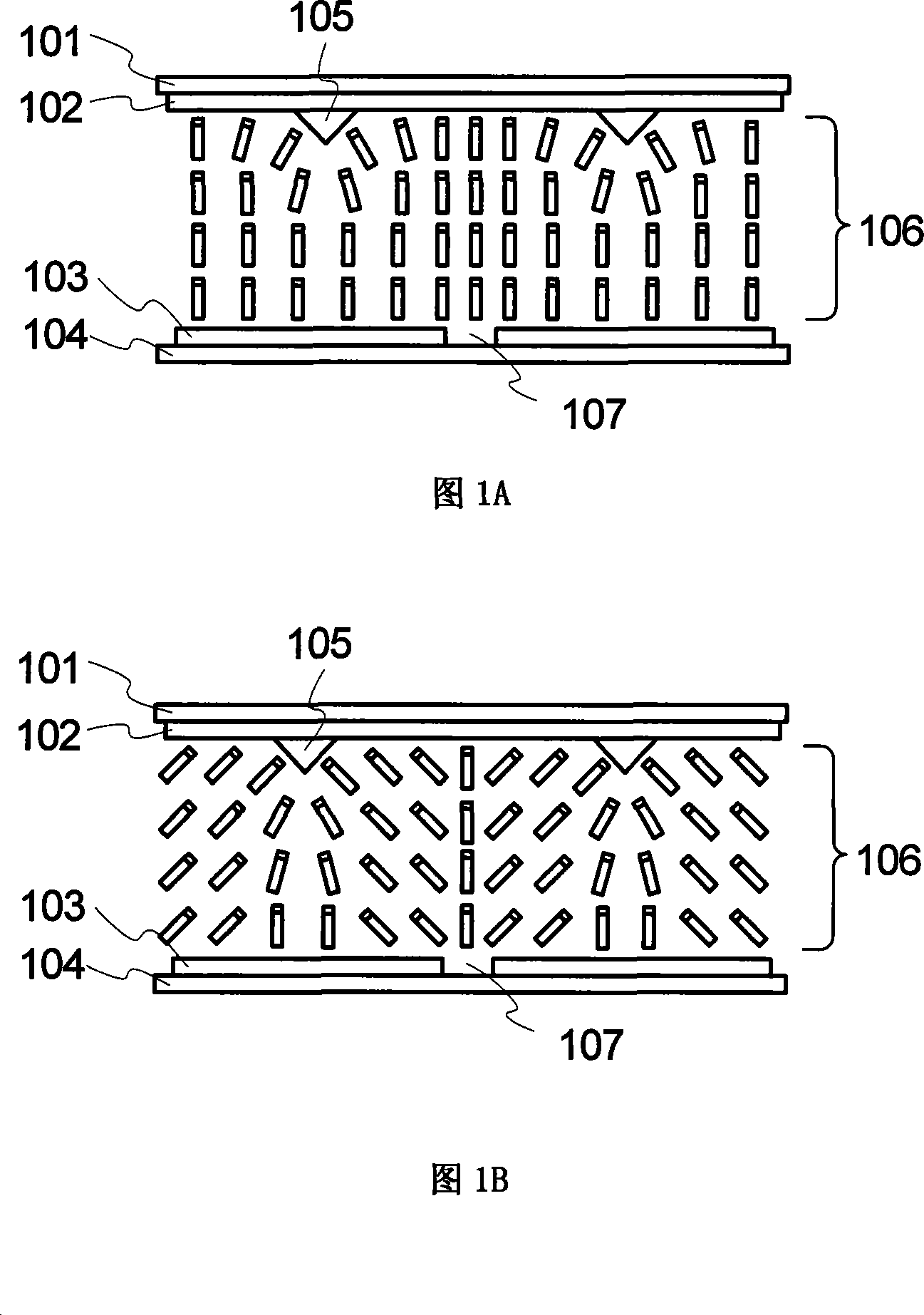
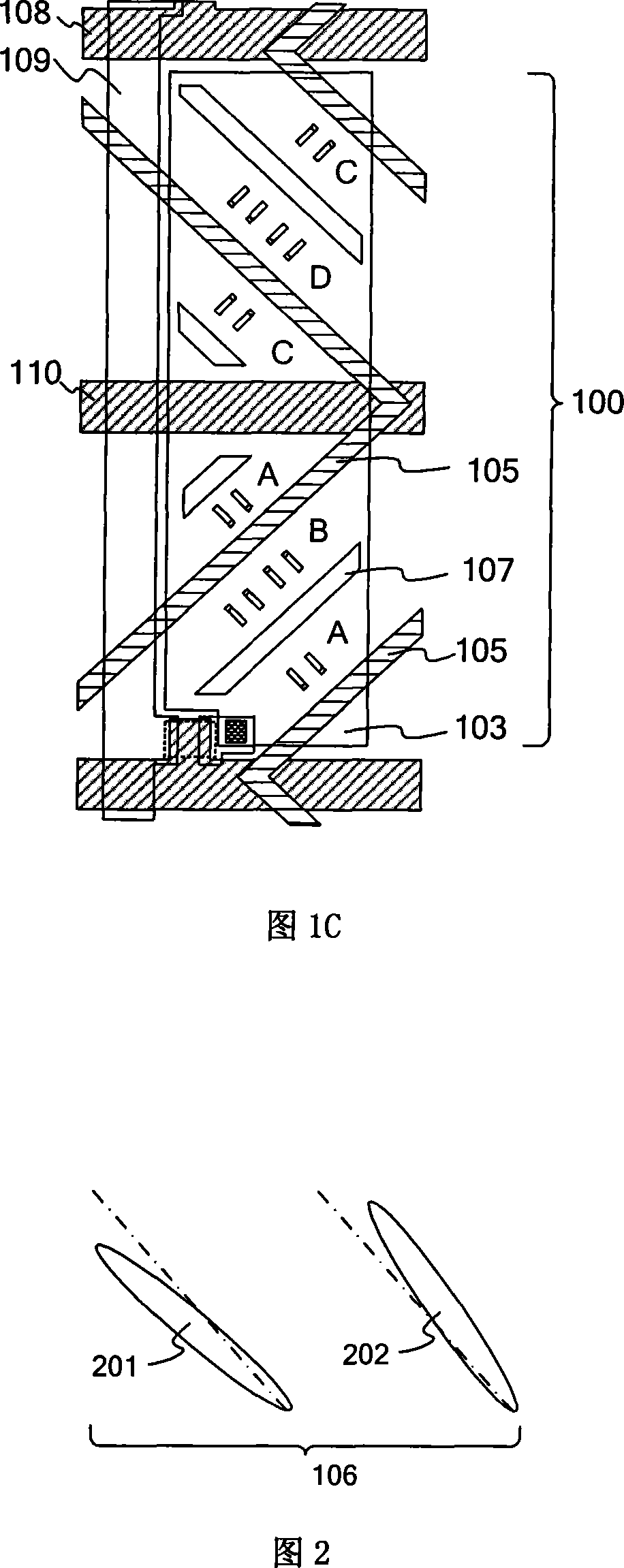
[0052] 8 is a schematic structural diagram of a pixel circuit used in a vertical alignment mode liquid crystal display device in an embodiment of the present invention; FIG. 10A is a schematic diagram of a pixel planar structure of a liquid crystal display device using a pixel circuit in the first embodiment of the present invention; FIG. 10B is a schematic diagram 10A is a schematic cross-sectional structure along the AA' direction; FIG. 10c is a schematic cross-sectional structure along the BB' direction in FIG. 10A.

[0053] This embodiment uses the structure of the multi-domain vertical alignment mode liquid crystal display device of FIG. 1. Referring to FIGS. 1 and 10, the vertical alignment mode liquid crystal display device of the present invention includes a first substrate 101, a second substrate 104, and A first conductive layer, a gate insulating layer, a second conductive layer, and a pixel electrode layer are sequentially formed on the second substrate 104. The gate s...

Embodiment 2

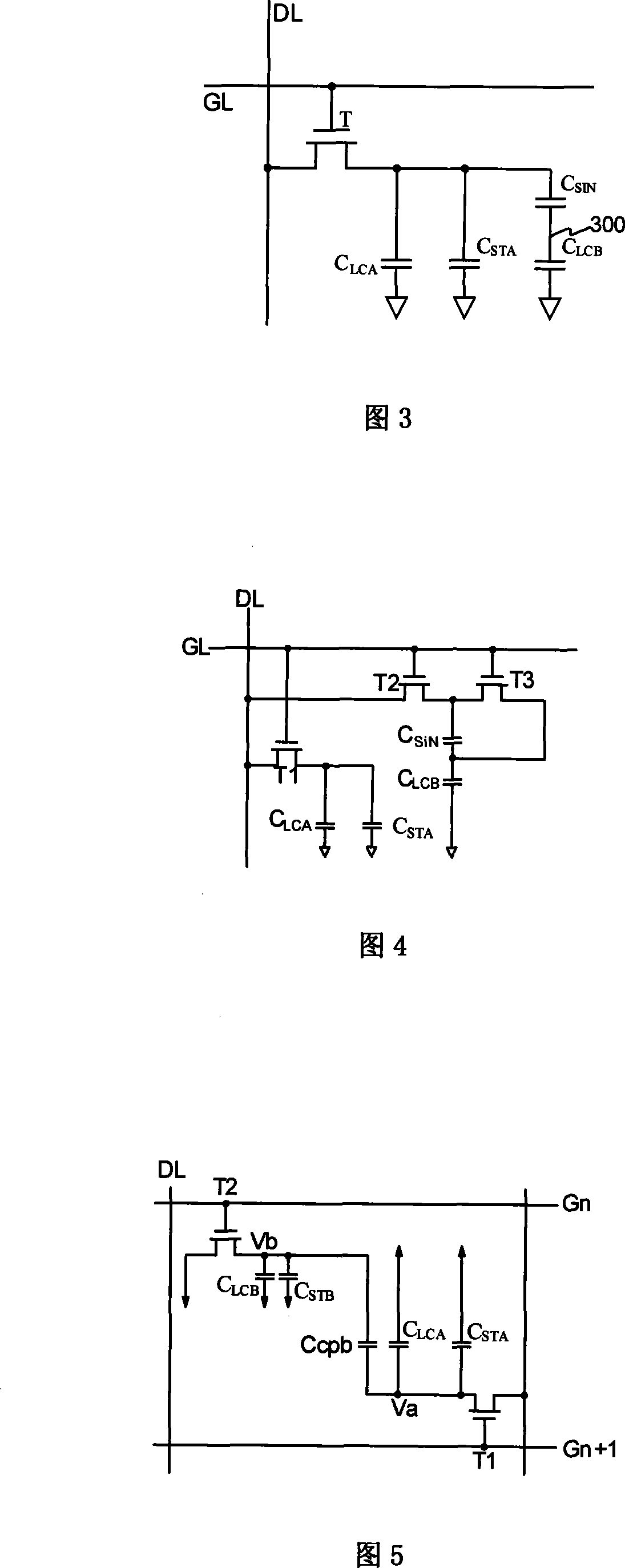
[0058] Referring to FIG. 9, the working principle is basically the same as the first embodiment. The difference is that when voltage data is written in the pixel, the first sub-pixel and the second sub-pixel are written with two TFTs respectively, that is, a fourth thin film transistor T4 is provided in the second sub-pixel to control the second sub-pixel. For pixel data writing, the fourth thin film transistor T4 is controlled by the gate scanning line Gn. Compared with the first embodiment, the second sub-pixel uses a thin film transistor T4 alone to control data writing. The process of capacitor discharge and voltage reset is basically the same as the first embodiment. However, the discharge process does not affect the first sub-pixel. If the pixel voltage value in the last frame of image is the same as or very close to the pixel voltage value of the current frame of image, the first sub-pixel and the second sub-pixel are voltage reset in the first embodiment, and the signal ne...


PUM


Abstract

The present invention discloses a vertical orientation type liquid crystal display device, which includes a plurality of pixels defined by crossing a grid scanning beam and a data line, each pixel is divided into at least a first sub-pixel and a second sub-pixel; and a plurality of pixel circuits connected to the grid scanning beam and the data line. The pixel circuit includes at least a first membrane transistor, a second membrane transistor, a third membrane transistor, a first sub-pixel capacitor, a second sub-pixel capacitor, a storage capacitor, and an additional capacitor. The storage capacitor is connected with the first sub-pixel capacitor in parallel to keep the data signal voltage transmitted through the data line. The additional capacitor is connected with the second sub-pixel capacitor in series, is connected with the second membrane transistor in parallel. One terminal of the second sub-pixel capacitor is connected with the second electrode of the third membrane transistor electrically. The second membrane transistor and the third membrane transistor are controlled by the previous row of grid scanning beam.

Description

Technical field [0001] The invention relates to a liquid crystal display device, in particular to a thin film transistor liquid crystal display device in a vertical alignment mode. Background technique [0002] The liquid crystal in the liquid crystal display device itself does not emit light. The liquid crystal display controls the light transmittance of the liquid crystal cell by controlling the twist of the liquid crystal molecules by an electric field, so as to achieve the purpose of display. Generally, in TFT-LCD (Thin Film Transistor Liquid Crystal Display), liquid crystal is enclosed between the upper and lower substrates. In a vertical alignment mode TFT-LCD, liquid crystal molecules are generally composed of a liquid crystal material with a negative dielectric constant and anisotropy. With reference to US Patent 6661488B1, when no voltage is applied to the upper and lower substrates of the liquid crystal display device, the liquid crystal molecules 106 are arranged perpe...

Claims


Application Information

Patent Timeline
IPC IPC(8): G02F1/1362G02F1/133G02F1/139G09G3/36
Inventor 李俊峰李喜峰
Owner NANJING CEC PANDA LCD TECH
Why Eureka
Try Eureka