Method for semiconductor device performance enhancement

a technology of semiconductor devices and enhancement methods, which is applied in the direction of semiconductor devices, basic electric elements, electrical appliances, etc., can solve the problems of degrading pmos performance, and achieve the effects of enhanced performance, enhanced performance, and enhanced performan

Inactive Publication Date: 2008-03-27
TAIWAN SEMICON MFG CO LTD
View PDF11 Cites 6 Cited by
  • Summary
  • Abstract
  • Description
  • Claims
  • Application Information

AI Technical Summary

Benefits of technology

[0007]Methods for manufacturing semiconductor devices with enhanced performance are provided. An exemplary embodiment of a method for manufacturing a semiconductor device with enhanced performance comprises: providing a semiconductor substrate with at least a PMOS device and at least an NMOS device thereon; forming a conformal first insulating layer overlying the NMOS and PMOS devices; forming a conformal second insulating layer overlying the first insulating layer; thinning the second insulating layer overlying the PMOS device to leave a portion of the second insulating layer, performing a first thermal treatment on the NMOS and PMOS devices; removing the second insulating layer overlying the NMOS device and the remaining portion of the second insulating layer overlying the PMOS device and thinning the first insulating layer overlying the NMOS and PMOS devices to leave a portion of the first insulating layer.
[0008]Another embodiment of a method for manufacturing semiconductor devices with enhanced performance comprises: preventing charge accumulation by providing a semiconductor substrate including a front side and a rear side; simultaneously forming a first insulating layer overlying the front side and a second insulating layer overlying the rear side; forming a third insulating layer overlying the first insulating layer; removing the third insulating layer by a wet etching step; and loading the semiconductor substrate onto an e-chuck stage, wherein the second insulating layer is between the e-chuck stage and the semiconductor substrate.
[0009]Another embodiment of a method for manufacturing semiconductor devices with enhanced performance comprises: preventing charge accumulation by providing a semiconductor substrate including a front side and a rear side, wherein at least a PMOS device and at least an NMOS device are formed on the front side; simultaneously forming a conformal first insulating layer overlying the NMOS and PMOS devices and a second insulating layer overlying the rear side; forming a conformal third insulating layer overlying the first insulating layer; thinning the third insulating layer overlying the PMOS device to leave a portion of the third insulating layer, performing a first thermal treatment on the NMOS and PMOS devices; removing the third insulating layer overlying the NMOS device and the remaining portion of the third insulating layer overlying the PMOS device and thinning the first insulating layer overlying the NMOS and PMOS devices to leave a portion of the first insulating layer.

Problems solved by technology

PMOS performance, however, is still degraded.

Method used


Image

  • Method for semiconductor device performance enhancement
  • Method for semiconductor device performance enhancement
  • Method for semiconductor device performance enhancement

Examples


first embodiment

[0025]FIG. 2a˜2i are sectional views showing a first embodiment of fabrication of a CMOS device.

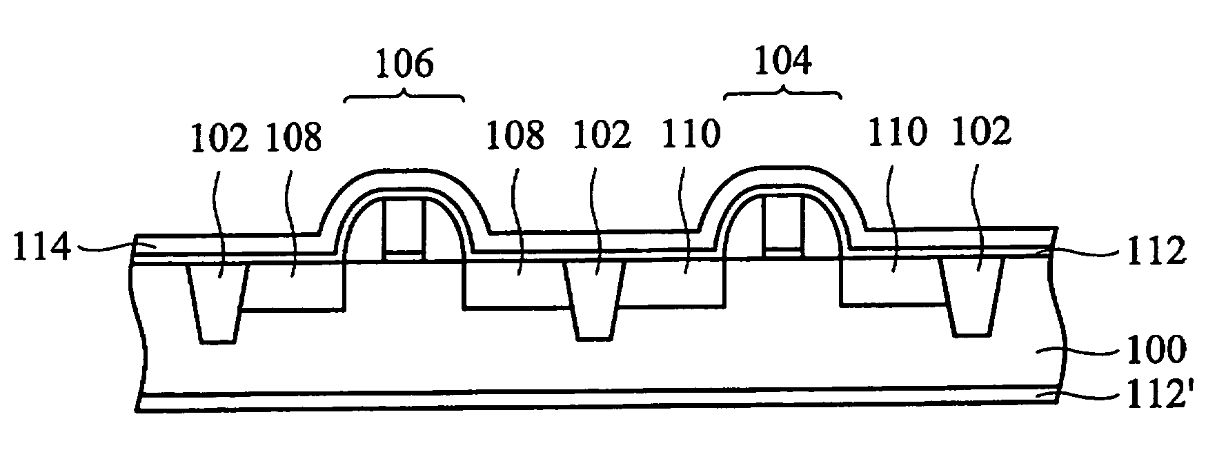
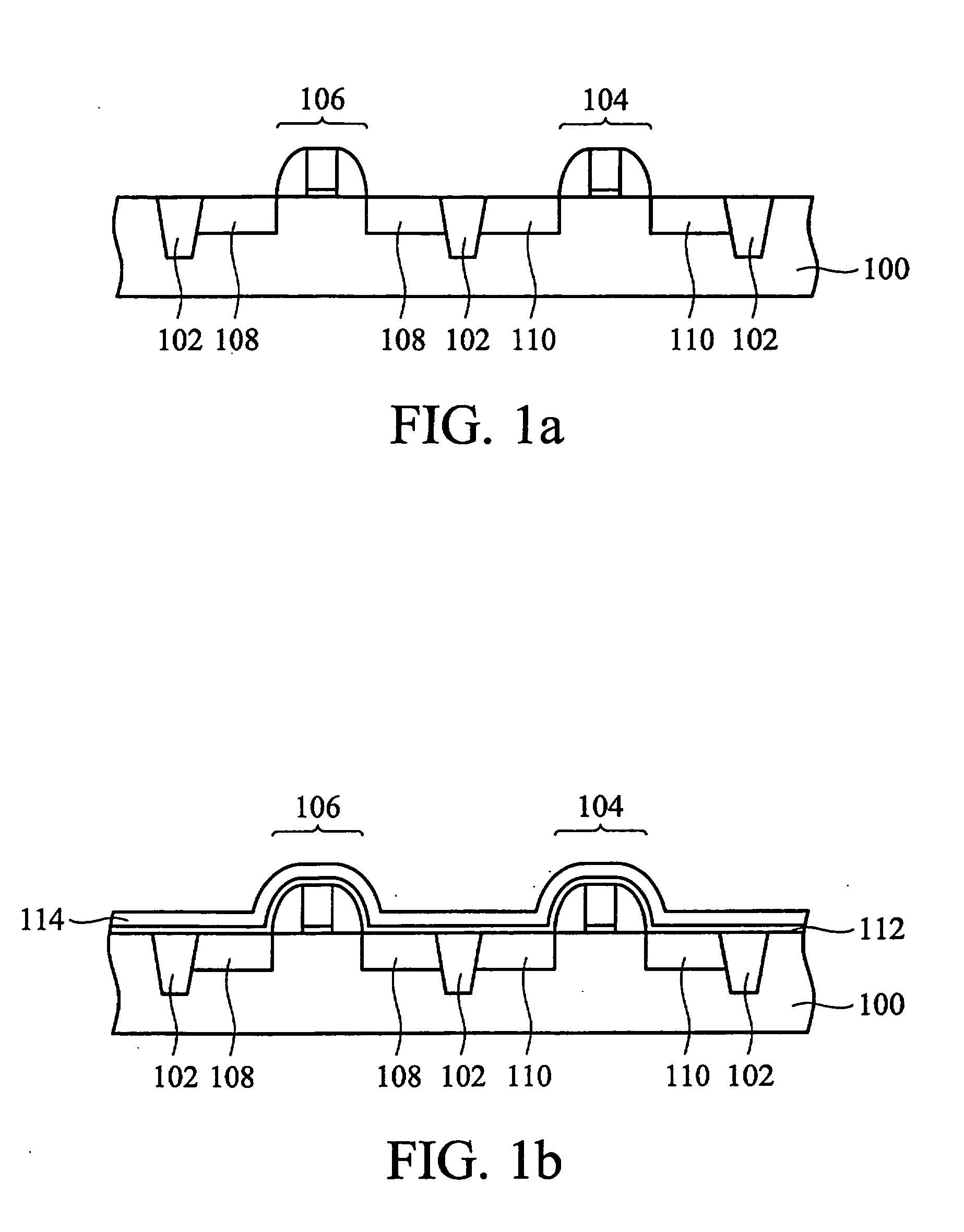
[0026]As shown in FIGS. 2a, 2b and 2c, the elements or procedures using the same numerals are similar to (or the same as) those shown in the FIG. 1a˜1 and thus are not described again. In the first embodiment, the oxide layer 112 is a TEOS oxide layer of 80 angstroms in thickness and the silicon nitride layer 114 has a thickness greater than 200 angstroms. The oxide layer 112 and the silicon nitride layer 114 are formed at 200˜800□. The formation thereof is as described in the comparative example. In other embodiments, the oxide layer 112 has a thickness between 10 and 300 angstroms.

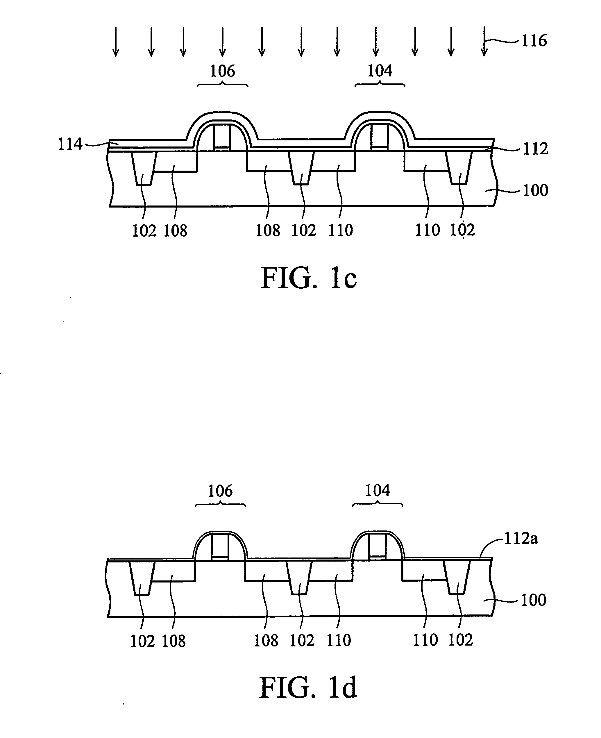
[0027]As shown in FIG. 2d, a photoresist layer 202 is subsequently disposed on the PMOS device 104 and NMOS device 106 and the upper surface of the semiconductor substrate 100. An exposure step 204 is then performed on the photoresist layer 202 overlying the overall semiconductor substrate 100 prior to a devel...

second embodiment

[0035]The second embodiment is similar to the first embodiment, except that a silicon nitride layer 114 of 350 angstroms is employed (referring to FIG. 2a). Specifically, the second embodiment is suitable for 65 nm generation and the thickness of the silicon nitride layer 114 can be between 200-350 angstroms depending on a pitch between the PMOS and NMOS devices.

third embodiment

[0036]The third embodiment is similar to the first embodiment, except that a silicon nitride layer 114 of 500 angstroms is employed (referring to FIG. 2a). Specifically, the third embodiment is suitable for the 90 nm generation and the thickness of the silicon nitride layer 114 can be between 200˜500 angstroms depending on a pitch between the PMOS and NMOS devices.

[0037]The following fourth embodiment comprises a method for preventing charge accumulation in a semiconductor device. The charge is generated from an electrostatic chuck (e-chuck) stage of an apparatus and may accumulate within the semiconductor substrate of the described comparative example or embodiments, affecting the reliability of the semiconductor device.


PUM


Abstract

A method of manufacturing a semiconductor device is disclosed. The method provides a semiconductor substrate with at least a PMOS device and at least an NMOS device thereon. A first insulating layer is formed overlying the NMOS and PMOS devices. A second insulating layer is formed overlying the first insulating layer. The second insulating layer overlying the PMOS device is thinned to leave portion of the second insulating layer. A first thermal treatment is performed on the NMOS and PMOS devices. The second insulating layer overlying the NMOS device and the remaining portion of the second insulating layer overlying the PMOS device are removed and the first insulating layer overlying the NMOS and PMOS devices is thinned to leave a remaining portion thereof.

Description

BACKGROUND OF THE INVENTION[0001]1. Field of the Invention[0002]The invention relates to fabrication of a semiconductor device, and more particularly to fabrication of a CMOS device.[0003]2. Description of the Related Art[0004]To enhance NMOS performance without PMOS degradation in a semiconductor device, CMOS and PMOS devices are typically formed with tensile and compressive stresses, respectively. U.S. Pub. No. 2004 / 0104405 A1 to Huang et al. describes a CMOS device having at least one PMOS device comprising a first stress layer e.g. a compressive stress layer thereon and at least one NMOS comprising a second stress layer e.g. a tensile stress layer thereon, thus the mobility of holes and electrons within the CMOS device is improved. U.S. Pub. No. 2004 / 0159834 A1 to Huang et al. describes that adoption of a strained silicon layer facilitates fabrication efficiency of devices. U.S. Pub. No. 2006 / 0014340 A1 to Hisakazu et al. describes a semiconductor device comprising at least one ...

Claims


Application Information

Patent Timeline
Patent Type & Authority Applications(United States)
IPC IPC(8): H01L21/8238
CPCH01L21/823807H01L29/7843H01L21/823842H01L21/823814
Inventor CHUANG, HARRYTHEI, KONG-BENGCHENG, CHUNG-LONGCHUNG, SHENG-CHENGUO, WEN-HUEIKAO, JUNG-HUICHEN, RYAN CHIA-JENLIANG, MONG-SONG
Owner TAIWAN SEMICON MFG CO LTD
Why Eureka
Try Eureka