Solid image capturing device including CMOS image sensor

一种固体摄像装置、像素的技术,应用在固体图像信号发生器、图像通信、图片信号发生器等方向,能够解决RGB信号色再现性变差、没有进行使用W像素信号处理、W信号立即饱和等问题

Inactive Publication Date: 2008-07-16
KK TOSHIBA
View PDF5 Cites 25 Cited by
  • Summary
  • Abstract
  • Description
  • Claims
  • Application Information

AI Technical Summary

Problems solved by technology

[0005] However, since the W pixel is highly sensitive, there is a problem in that the W signal obtained from the W pixel is immediately saturated, or there is a problem in color reproducibility because the Y signal (brightness signal) = W signal
However, if the original Y signal is not generated according to the ratio of Y=0.59G+0.3R+0.11B, the color reproducibility of the RGB signal generated from the YUV signal will deteriorate
Furthermore, in the above-mentioned patent documents, effective signal processing using W pixels is not performed.

Method used


Image

  • Solid image capturing device including CMOS image sensor
  • Solid image capturing device including CMOS image sensor
  • Solid image capturing device including CMOS image sensor

Examples


Embodiment Construction

[0025] Hereinafter, an enhancement type CMOS image sensor as a solid-state imaging device according to an embodiment of the present invention will be described with reference to the drawings. In the description, in all the drawings, common reference numerals are assigned to common parts.

[0026] [First Embodiment]

[0027] First, a CMOS image sensor according to a first embodiment of the present invention will be described.

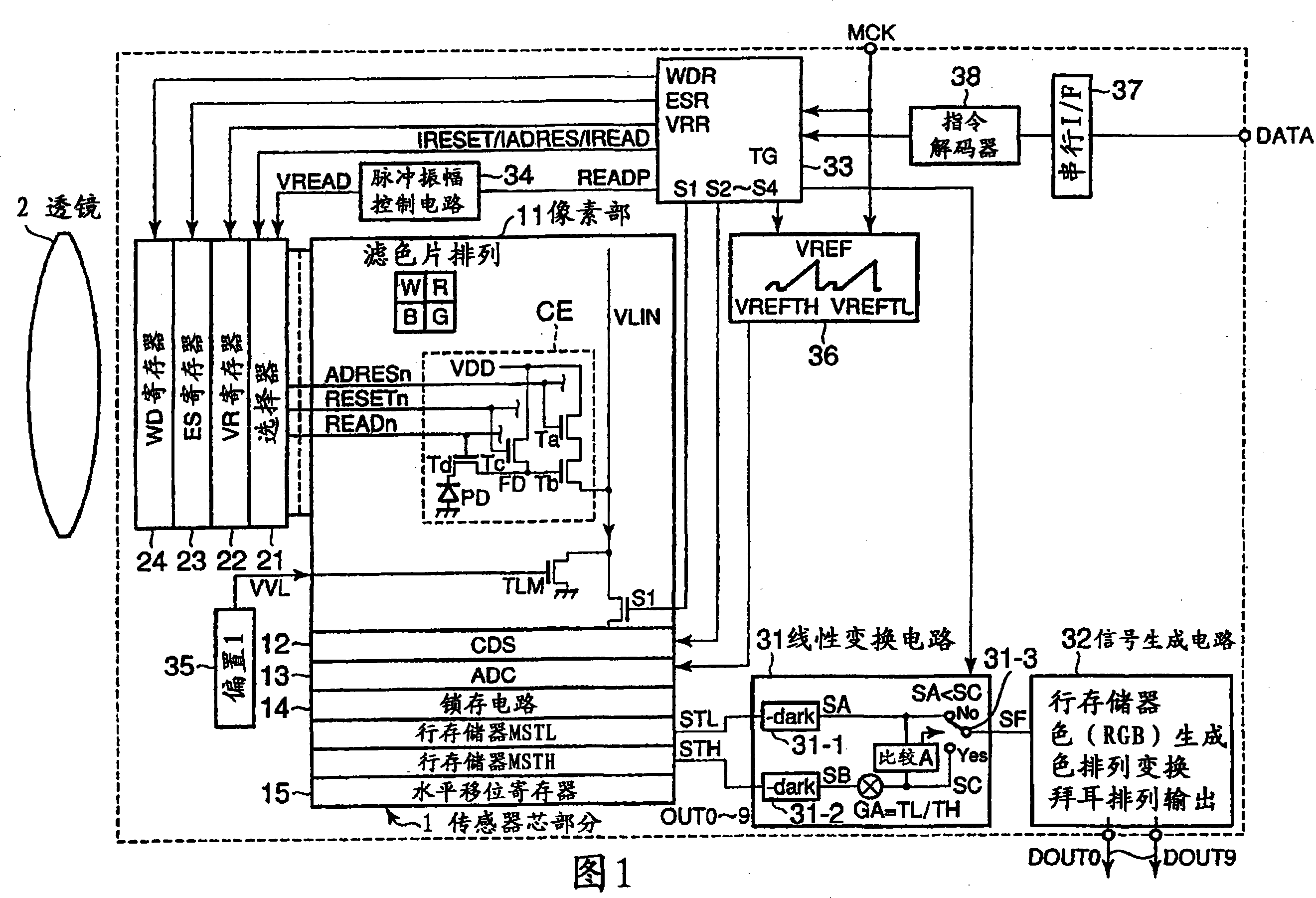
[0028] FIG. 1 is a block diagram showing a schematic configuration of a CMOS image sensor according to a first embodiment.

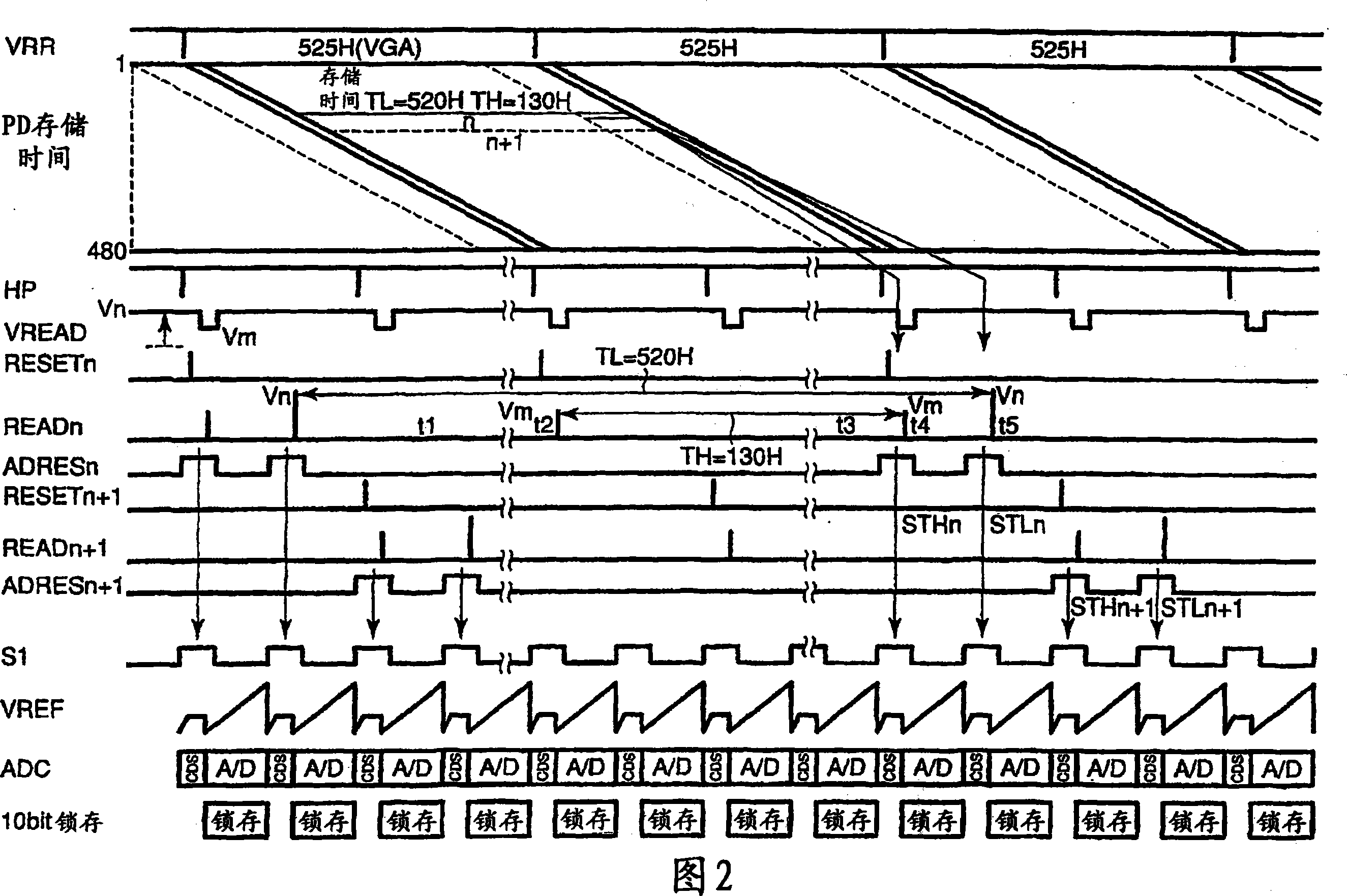
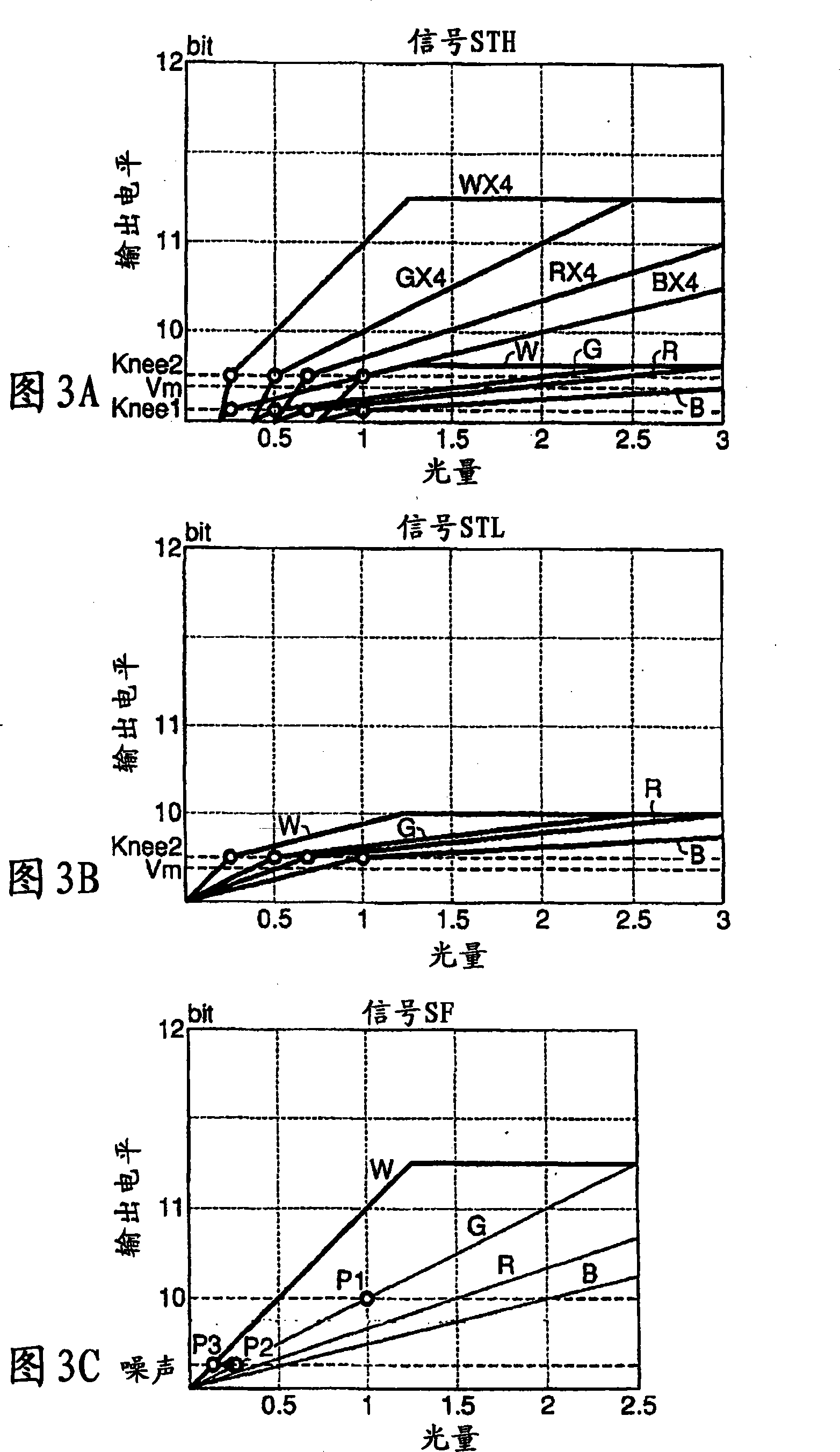
[0029] In the sensor core section 1, a pixel section 11, a column type noise canceling circuit (CDS) 12, a column type analog-to-digital converter (ADC) 13, a latch circuit 14, and two line memories are arranged. (1st row memory MSTH, 2nd row memory MSTL), horizontal shift register 15, and the like.

[0030] In the pixel portion 11 , light is incident through the lens 2 , and charges corresponding to the amount of the incident l...


PUM


Abstract

The present invention provides a solid camera shooting device containing CMOS type image sensor. In a pixel part, setting units in line and row on a semiconductor substrate to store signal charges obtained by implementing photoelectricity transformation to light incident to a photoelectricity transforming component, and to output voltage corresponding to the stored signal charge. Setting color filters of W, R, G, B separately on the units, and transforming analog signals exported from the Wpixel, R pixel, G pixel as well as B pixel to digital signals by an analog / digital transformation circuit, and outputting W, R, G, B signals separately, as well as controlling saturated signal quantity of the W signal by a saturated signal quantity control circuit, moreover, outputting the R, G, B signals corrected by a signal generating circuit (32) using the W signal exported from the AD transfromation circuit and the R, G, B signals.

Description

[0001] (Cross-reference to related application) [0002] This application is based on and claims priority from prior Japanese Patent Application No. 2007-000718 filed on January 5, 2007, the entire contents of which are incorporated herein by reference. technical field [0003] The present invention relates to a solid-state imaging device, and relates to a CMOS image sensor used in, for example, a mobile phone with an image sensor, a digital camera, a video camera, and the like. Background technique [0004] For color filters used in image sensors, various arrangements from complementary color filters to primary color Bayer arrangements have been proposed together with signal processing methods thereof. In image sensors, the miniaturization of pixels has progressed in recent years, and the 2μm generation has been put into practical use, and development of 1.75μm pixels or 1.4μm pixels is also underway. In fine pixels of 2 μm or less, since the amount of incident light is gr...

Claims


Application Information

Patent Timeline
Patent Type & Authority Applications(China)
IPC IPC(8): H04N9/04H04N5/232H04N5/335H04N5/355H04N5/369H04N5/374H04N5/378H04N9/07
CPCH04N9/045H04N5/35581H04N25/583H04N25/589H04N23/84H04N25/133H04N25/135
Inventor 江川佳孝本多浩大饭田义典伊藤刚
Owner KK TOSHIBA
Why Eureka
Try Eureka