

Conductive layer structure for chip encapsulation module and its making method
A chip packaging and conductive layer technology, which is applied in semiconductor/solid-state device manufacturing, circuits, electrical components, etc., can solve the problems of easy oxidation of conductive layers, achieve the effects of suppressing noise, avoiding contact, and improving EMI protection performance
Inactive Publication Date: 2010-11-10
XINTEC INC
View PDF0 Cites 0 Cited by
- Summary
- Abstract
- Description
- Claims
- Application Information
AI Technical Summary
Problems solved by technology
In view of this, the main purpose of the present invention is to provide a conductive layer structure and related manufacturing method that can solve the problem of easy oxidation of the conductive layer of the chip package module, improve EMI protection performance, and effectively suppress noise
Method used
View moreImage
Smart ImageViewing Examples

Examples
Embodiment Construction
Login to View More PUM
 Abstract
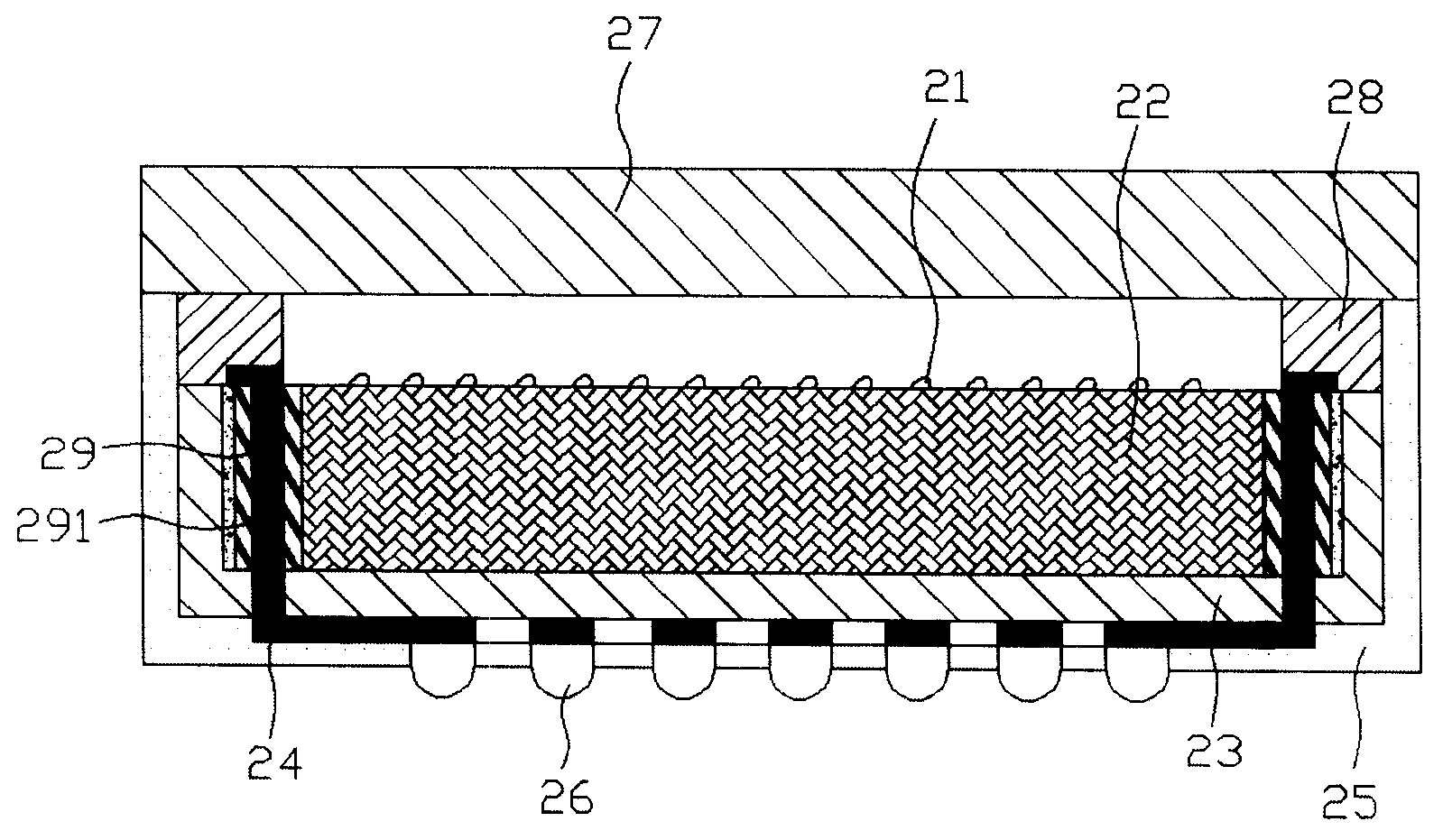
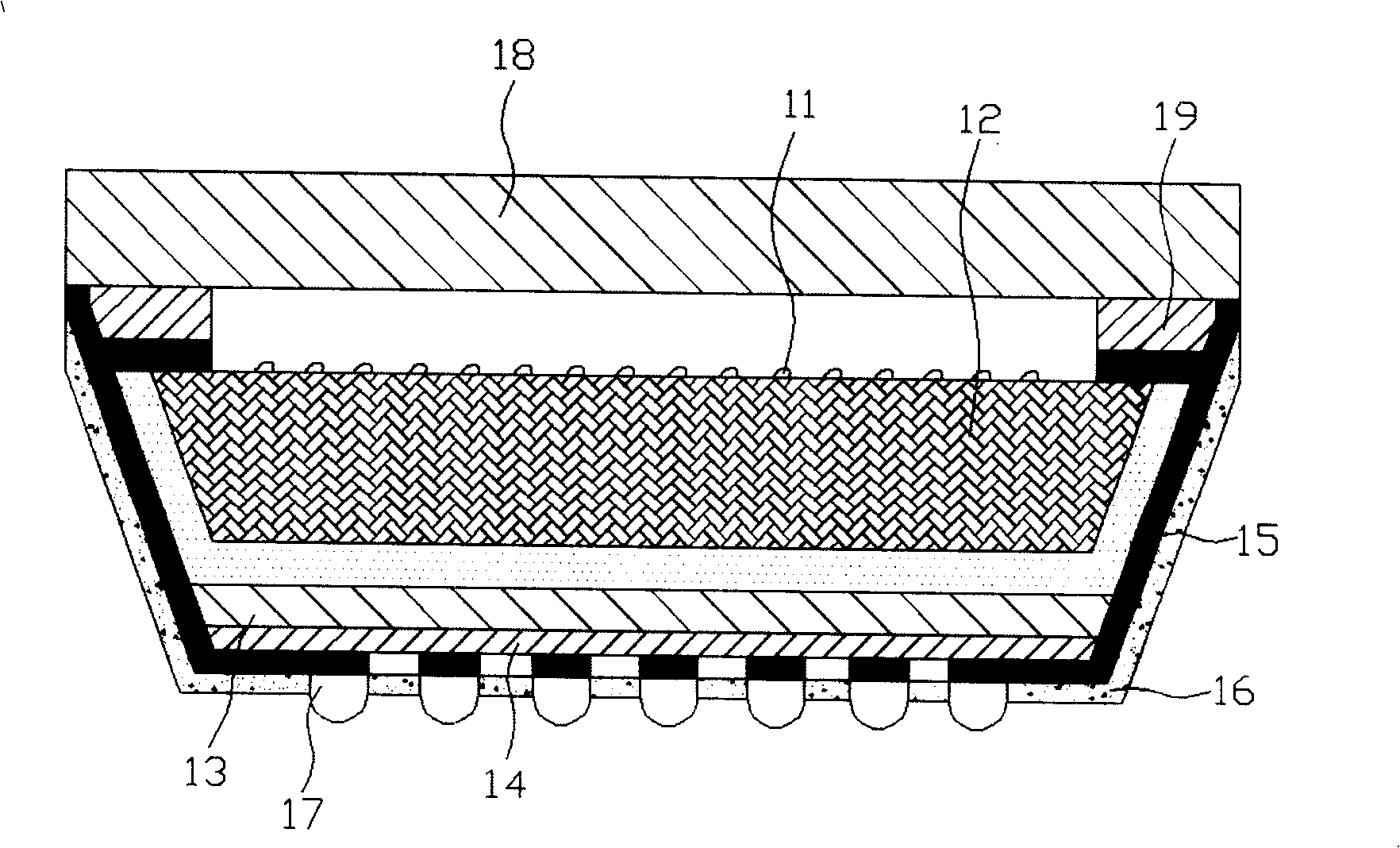
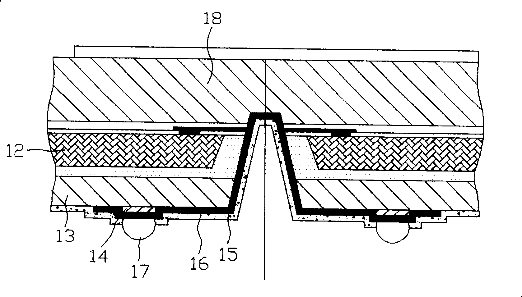
The invention provides a conductive layer structure on a chip packaging module and a method for manufacturing the chip packaging module. The method mainly comprising the following steps of: drilling at least one through hole to the top of a wafer at the bottom of an insulation layer of the chip packaging module, arranging insulation materials on the inner wall of each through hole to allow a conductive layer arranged at the periphery of the insulation layer to extend to the above of the wafer and then arranging a solder mask and a circuit pin so as to constitute a conductive layer structure which can be covered entirely to prevent oxidation, can enhance EMI protection performance and suppress noise effectively. The conductive layer structure not only can solve the problem that the conductive layer of the prior chip packaging module is easy to corrode due to oxidation, but also can make the conductive layer obtain better EMI shielding at the position close to other electronic elements and further enhance the EMI protection performance of the whole chip packaging module and effectively suppress the noise of the chip packaging module; meanwhile, the conductive layer structure can avoid 'T CONTACT' type contact to be more stable.
Description
Conductive layer structure of chip packaging module and manufacturing method thereof technical field The invention relates to a chip packaging module, especially improving the conductive layer structure of the chip packaging module, aiming to provide a conductive layer structure that is completely covered to prevent oxidation, improve EMI protection performance and effectively suppress noise. Background technique In recent years, due to the requirements of light weight and miniaturization of electronic products, the assembly and construction technology of electronic components has gradually developed towards the goal of lightness, thinness, shortness and smallness. The capability of / O signal and current, and the function of providing heat dissipation and protecting the photosensitive chip must be packaged to form an integrated chip package module. The image sensor shown in Figure 1 is taken as an example, which can be regarded as one of the typical modular chip packaging...
Claims
Login to View More Application Information
Patent Timeline
 Patent Type & Authority Patents(China)
IPC IPC(8): H01L23/552H01L23/48H01L21/50H01L21/60
CPCH01L2224/11H10K30/88
Inventor 刘建宏
Owner XINTEC INC