Redundant clock signal commutation circuit and method

A clock signal switching and clock signal technology, applied in the field of computer communication, can solve the problems of system business interruption, insurmountable, etc., to ensure the effect of not being interrupted

Inactive Publication Date: 2008-09-10
ZTE CORP
View PDF0 Cites 5 Cited by
  • Summary
  • Abstract
  • Description
  • Claims
  • Application Information

AI Technical Summary

Problems solved by technology

The switching method in the prior art cannot overcome the impact on the system caused by the time difference of the switching action caused by the loss of the main clock signal CLK1A (assuming that the system selects CLK1A as the main clock signal) to the S1 switch

Method used


Image

  • Redundant clock signal commutation circuit and method
  • Redundant clock signal commutation circuit and method
  • Redundant clock signal commutation circuit and method

Examples


Embodiment Construction

[0020] The present invention will be further described in detail below by taking two redundant clock signals as an example and in conjunction with the accompanying drawings.

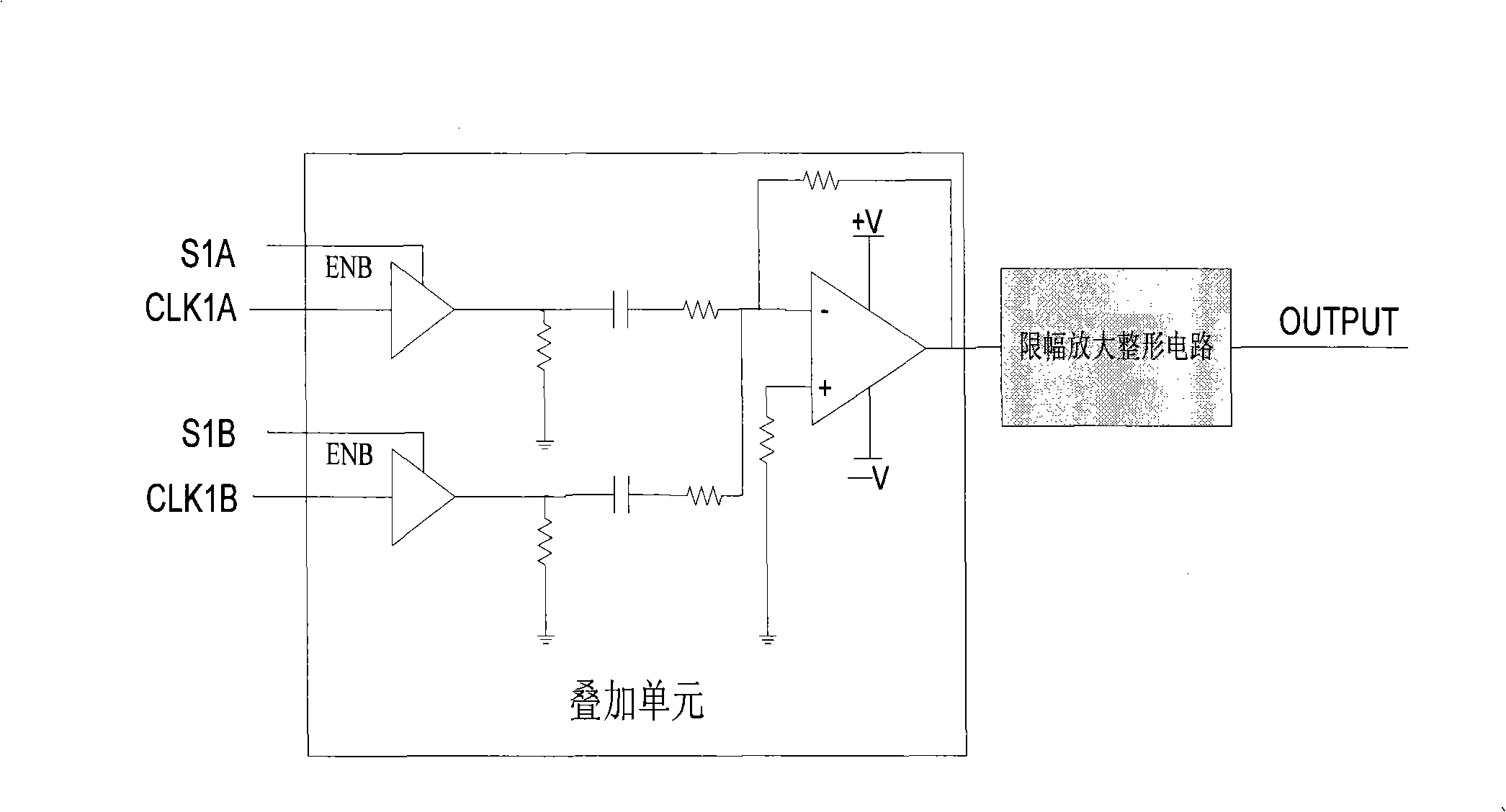
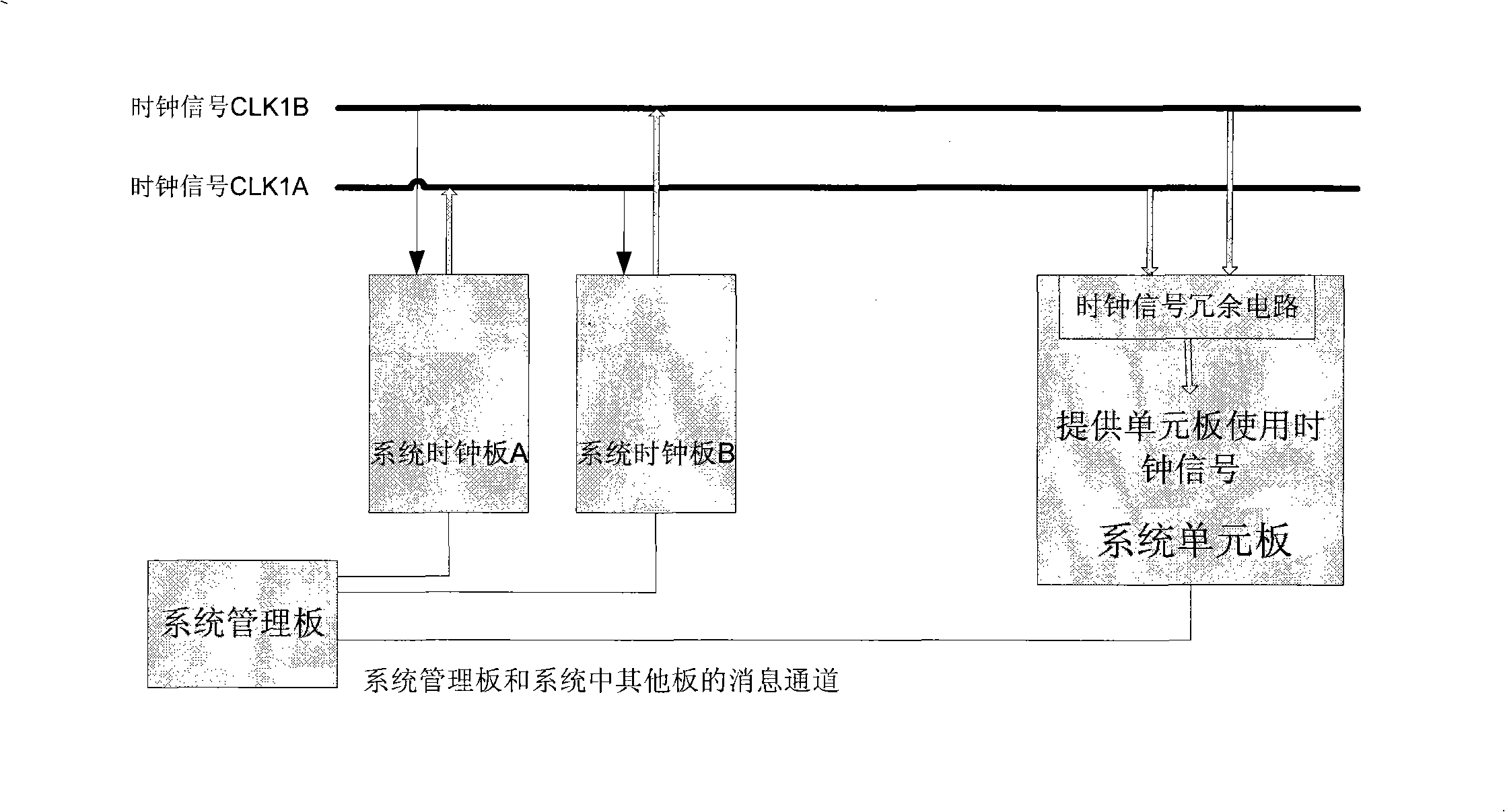
[0021] like figure 2 In the redundant clock signal switching circuit shown, CLK1A and CLK1B are mutually redundant clock signals input to a single board (or system unit board); S1A and S1B are control terminals for gating these two clock signals. The two clock signals are respectively connected to the input ends of the clock signal superimposition unit, and are superimposed by the clock signal superposition unit. figure 2 The shown two clock signals use a reverse summation circuit to superimpose the two clock signals. In specific implementation, other summation circuits or logic gate circuits can also be used to realize the superposition processing of multiple redundant clock signals. The signal output by the superposition unit is input to the single board or the unit board after being limited, amplif...


PUM


Abstract

The invention discloses a redundancy clock signal switching circuit and a method, clock signals with a plurality of lines in the circuit are respectively connected with an input end of a clock signal overlapping unit, the clock signals with a plurality of lines are output as the clock signal of a single plate or an unit plate after the overlapping processing by the clock signal overlapping unit; and each line of clock signal is carried out the on-off control by the corresponding switching control end. The usage of the switching circuit and the method which are proposed by the invention can not affect the continuity which is supplied to the single plate clock once the clock signals are turned off due to the faults or needs, thus ensuring no interruption of the business of the system.

Description

technical field [0001] The invention relates to the field of computer communication, more specifically to a switching circuit and a method for a single board to receive redundant clock signals in a computer communication hardware platform. Background technique [0002] There are many ways to realize the redundant processing technology of the system clock signal in the current communication hardware platform. According to the single board (or unit) that receives the system clock in the system, there are several input channels for the same clock signal. can be roughly divided into two categories: [0003] 1) For the same clock signal of the system, the single board (or unit) that needs to receive the system clock can only have one input at any time. In this case, the switching of redundant clock signals in system design is generally placed at the clock signal sending end. [0004] 2) For the same clock signal of the system, the single board (or unit) that needs to receive th...

Claims


Application Information

Patent Timeline
IPC IPC(8): G06F1/04
Inventor 邵贵阳赵阳
Owner ZTE CORP
Why Eureka
Try Eureka