Inverse fuse wire and memory cell without ability to cause non-linear current after fusing

A non-linear current and storage unit technology, applied in the direction of electrical components, circuits, electric solid-state devices, etc., can solve the problems that the sensing circuit cannot correctly detect whether the storage unit is programmed, and the reliability of the one-time programming memory.

Inactive Publication Date: 2008-09-24
UNITED MICROELECTRONICS CORP
View PDF0 Cites 74 Cited by
  • Summary
  • Abstract
  • Description
  • Claims
  • Application Information

AI Technical Summary

Problems solved by technology

The p / n junction will cause a non-linear current after the anti-fuse is blown, and the non-linear current will make the sensing circuit of the one-time programming memory unable to correctly detect whether the memory cell is programmed, which affects the reliability of the one-time programming memory Have a great impact

Method used


Image

  • Inverse fuse wire and memory cell without ability to cause non-linear current after fusing
  • Inverse fuse wire and memory cell without ability to cause non-linear current after fusing
  • Inverse fuse wire and memory cell without ability to cause non-linear current after fusing

Examples


Embodiment Construction

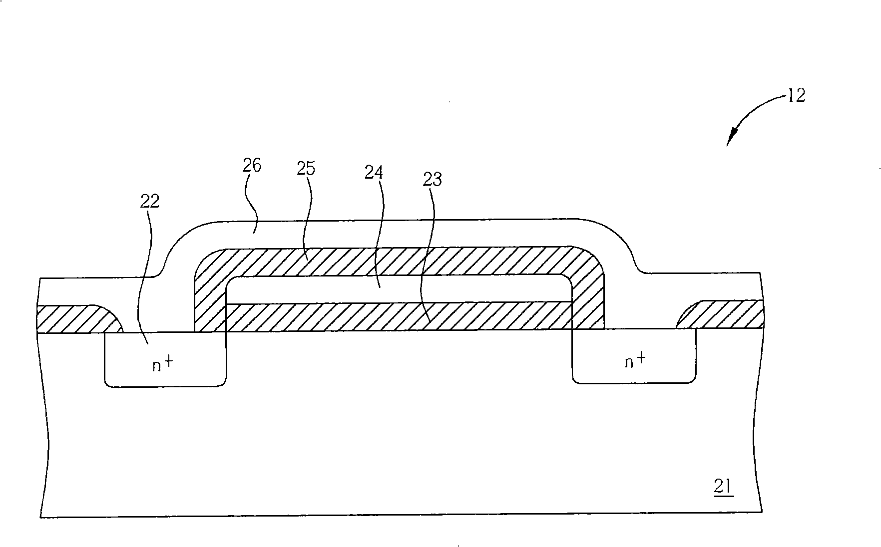
[0033] Please refer to Figure 4 , Figure 4It is a cross-sectional view of the antifuse 30 according to the first embodiment of the present invention. The antifuse 30 includes an n-type substrate 31 , two p+ doped regions 32 , a p-type channel 37 , a dielectric layer 33 , a conductive layer 34 , an insulating layer 35 and a wire 36 . Two p+ doped regions 32 and a p-type channel 37 are implanted from above the n-type substrate 31 to form in the n-type substrate 31 . The dielectric layer 33 is silicon dioxide and formed on the n-type substrate 31 to isolate the n-type substrate 31 from the conductive layer 34 . The conductive layer 34 is polysilicon formed on the dielectric layer 33 . The insulating layer 35 is silicon dioxide and is used to isolate the conductive layer 34 and the wire 36 . The wire 36 is a metal wire, and is coupled to the two p+ doped regions 32 through the contact window. A first end of the antifuse 30 is a conductive layer 34 , a second end of the anti...


PUM


Abstract

The anti-fuse is formed by a transistor of a channel with doping carriers, which can not lead to the nonlinear electric current after fusing and can be used for a memory cell of a memorizer for programming of expression of first degree. The memorizer for programming of expression of first degree adopts a P-shaped transistor and an N-shaped transistor for programming for the anti-fuse. As the anti-fuse is provided with the channel with doping carriers, after the anti-fuse is fused, the electric current can not flow through the P/N knob between two doping regions and basements to form a nonlinear electric current, thus leading the memory cell to be programmed correctly.

Description

technical field [0001] The invention relates to an antifuse, in particular to an antifuse which will not cause nonlinear current after fusing. Background technique [0002] Anti-fuse (anti-fuse) is a kind of component that is short-circuited at both ends after fusing relative to the fuse. Generally, the two ends of the antifuse are separated by a silicon oxide-like insulating layer. In the disconnected state, there is a high resistance value between the two ends of the antifuse, and the insulating layer is broken down by applying a high voltage. The two ends of the antifuse form a short circuit, which has a low resistance value of about 5-25K ohms, so the antifuse is very suitable for use in programming memories. The programming memory using the anti-fuse can provide better protection in terms of confidentiality due to its one-time programming (One-Time Programming, OTP) feature. At present, the commonly used antifuse is to use the structure of complementary metal oxide se...

Claims


Application Information

Patent Timeline
Patent Type & Authority Applications(China)
IPC IPC(8): H01L23/525H01L27/112H01L27/115
Inventor 张光晔许兴仁何仲仁
Owner UNITED MICROELECTRONICS CORP
Why Eureka
Try Eureka