

Method and device for reducing offset voltage of Hall integrated circuit
An offset voltage, integrated circuit technology, applied in circuits, electrical components, electric solid devices, etc., can solve the problems of unpredictable and controllable offset voltage, and achieve good consistency, small Hall output voltage offset, and good matching. Effect
- Summary
- Abstract
- Description
- Claims
- Application Information
AI Technical Summary
Problems solved by technology
Method used
Image

Examples
no. 1 example
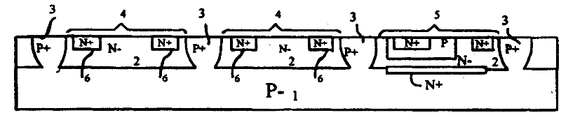
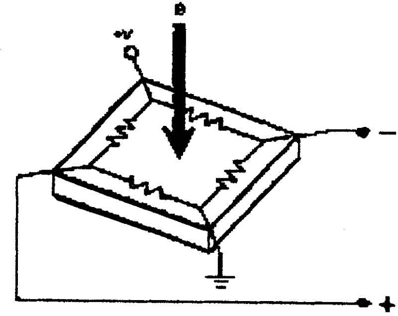
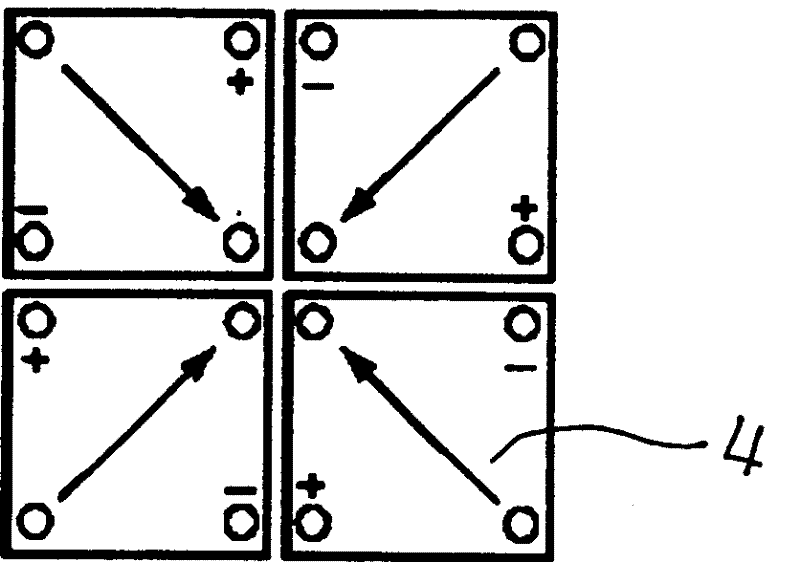
[0033] Fig. 6 shows a sectional view along the direction A-A of Fig. 5 . The same number in the figure represents the same area. A lightly doped N-type epitaxial layer 2 is grown on a semiconductor P-type base substrate 1 , and the epitaxial layer 2 is separated by heavily doped P-type isolation bands 3 into isolated epitaxial islands, that is, Hall cells 4 . Four identical Hall cells 4 connected in parallel form a Hall sensor and are located in the middle of the chip (FIG. 5).
no. 2 example
[0035] Figure 8 shows the layout design method and connection mode of the Hall unit 4 of the second embodiment. Compared with the first embodiment, the Hall unit 4 is rotated at an angle of 45 degrees, and the wider part is not shown in the figure. Epitaxial layer 2 and isolation zone 3.
no. 3 example
[0037] Figure 9 shows the layout design method and connection mode of the Hall unit 4 of the third embodiment. Compared with the second embodiment, it is only composed of three Hall units 4, and the Hall unit 4 is symmetrical to the center of a parallelogram Balanced setting, the wider epitaxial layer 2 and the isolation zone 3 are not drawn in the figure.
PUM
 Abstract
Description
Claims
Application Information