Picture edge dead point emendation method and device thereof
A technology for image edge and bad pixels, applied in the field of correction method and correction device for image edge bad pixels, capable of solving problems such as poor image data quality
- Summary
- Abstract
- Description
- Claims
- Application Information
AI Technical Summary
Problems solved by technology
Method used
Image
Examples
Embodiment Construction
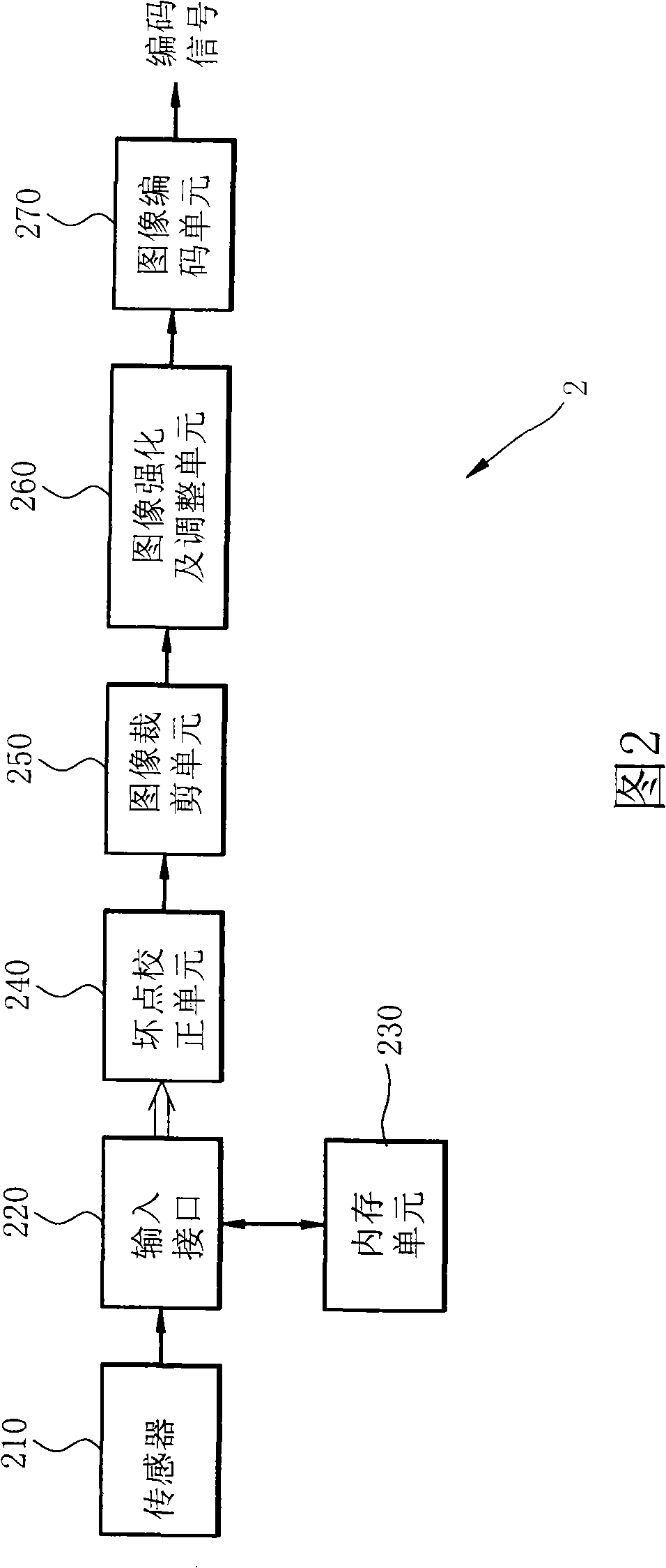
[0045] Please refer to FIG. 2 , which is a schematic block diagram of the device for correcting bad pixels at the edge of an image according to the present invention. The image edge defect correction device 2 of the present invention includes a sensor 210, an input interface 220, a memory unit 230, a defect correction unit 240, an image cropping unit 250, an image enhancement and adjustment unit 260 and an image encoding unit 270.
[0046] The input interface 220 is connected to the sensor 210 and the memory unit 230 for receiving image data (image frame) sensed by the sensor 210 to further scan pixels of each frame of detected image data. When the sensor 210 connected to the input interface 220 supports an image expansion function, the image data received by the input interface 220 may be expanded image data. In addition, the data generated by the input interface 220 processing the image data is temporarily stored in the memory unit 230 .
[0047] The dead point correction ...
PUM
 Abstract
Description
Claims
Application Information


