Single layer touch control sensing structure and touch control display panel using the same

A touch display panel and touch sensing technology, applied in the input/output process of data processing, instruments, electrical digital data processing, etc., can solve problems such as screen wear, sensor error judgment, poor light transmission, etc.

Inactive Publication Date: 2008-12-10
J TOUCH CORPORATION
View PDF1 Cites 26 Cited by
  • Summary
  • Abstract
  • Description
  • Claims
  • Application Information

AI Technical Summary

Problems solved by technology

Although this technology is simple, it still has the following disadvantages: First, the resistive touch panel has a two-layer structure, so it still has a certain thickness.
Second, the above-mentioned technology is also easy to cause screen wear and tear. If coatings are added to protect the screen or reduce reflection, it will cause poor light transmission.
Third, the hand-shadow effect (hand-shadow effect) is also easy to make the sensor judge wrong

Method used


Image

  • Single layer touch control sensing structure and touch control display panel using the same
  • Single layer touch control sensing structure and touch control display panel using the same
  • Single layer touch control sensing structure and touch control display panel using the same

Examples


Embodiment Construction

[0020] In order to have a further cognition and understanding of the features, purposes and functions of the present invention, the relevant detailed structure and design concept of the device of the present invention will be explained below, so that the review committee can understand the characteristics of the present invention, in detail The description states the following:

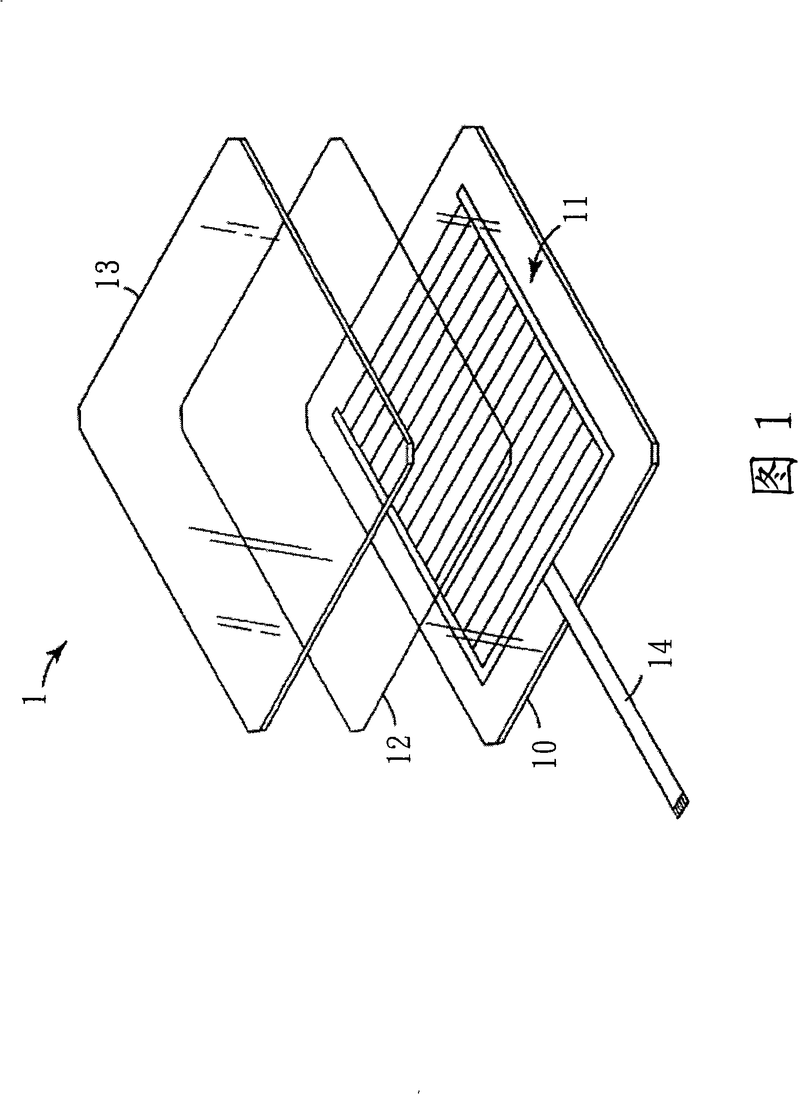
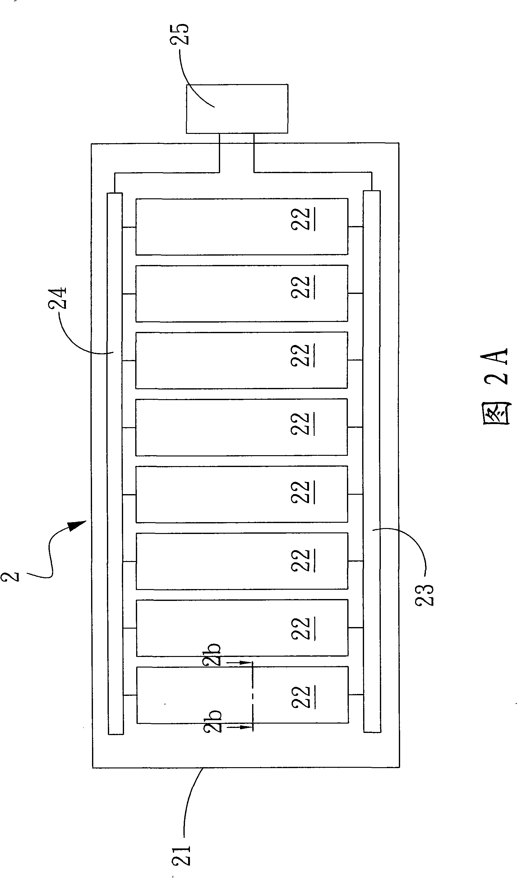
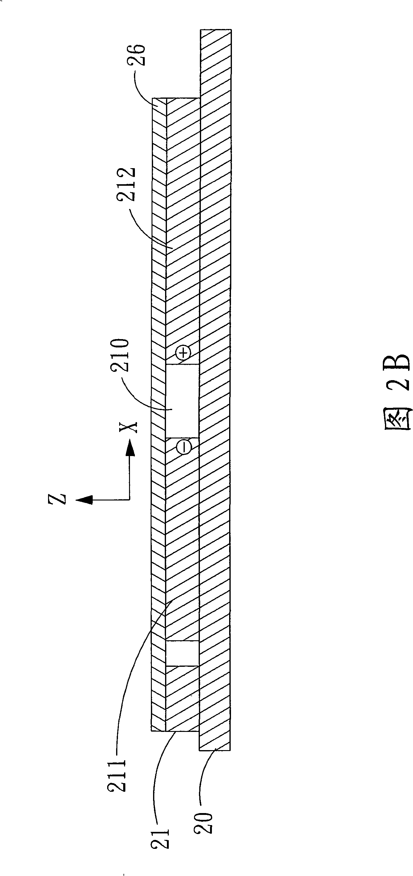
[0021] Please refer to FIG. 2A , which is a schematic diagram of an embodiment of a single-layer touch sensing structure of the present invention. The single-layer touch sensing structure 2 includes a conductive layer 21, which has a plurality of sensing blocks 22, and the sensing blocks 22 have multiple segments of grooves to divide the sensing blocks into A plurality of electrodes, any two adjacent electrodes can form a planar capacitance structure. The single-layer touch sensing structure 2 of the present invention is characterized in that only one conductive layer 21 can be used to complete the c...


PUM


Abstract

The invention provides a single-layer touch sensing structure comprising a conducting layer. The conducting layer is provided with at least one induction block. The induction block is provided with a plurality of grooves. The induction block is divided into a plurality of electrodes by the grooves. A plane capacitance structure is formed between two optional adjacent electrodes. Adopting the single-layer touch sensing structure, the invention further provides a touch display panel that comprises the conducting layer, a telecommunication circuit module and a display unit. The conducting layer is provided with a plurality of grooves and the induction block is divided into a plurality of electrodes. The telecommunication circuit module has electric connection with a plurality of electrodes. The display unit has coupling with the telecommunication circuit module to determine a touch position according to the capacitance change of the sensing area. The display unit is arranged below the conducting layer.

Description

technical field [0001] The present invention relates to a sensing structure and a touch panel, in particular to a single-layer touch sensing structure in which a plurality of planar capacitors are formed on a single-layer conductive layer and a touch display panel using the structure. Background technique [0002] Touch panels originated in the 1970s when the U.S. military developed them for military use. In the 1980s, the technology was transferred to civilian use, and then developed into various uses. Traditional electronic computing devices (such as computers) use peripheral devices such as keyboards or mice as input interfaces. However, these peripheral input devices are too large and difficult to carry, which is likely to cause a major obstacle to the thinning of electronic products. Due to the demand for thinner electronic devices, touch panels are gradually becoming more and more popular in portable electronic products. In addition, in addition to the application of ...

Claims


Application Information

Patent Timeline
Patent Type & Authority Applications(China)
IPC IPC(8): G06F3/044
Inventor 叶裕洲何炜轩
Owner J TOUCH CORPORATION
Why Eureka
Try Eureka