
Lateral DMOS device and method for fabricating the same

A conductive type, deep well technology, applied in semiconductor/solid-state device manufacturing, electric solid-state devices, semiconductor devices, etc., can solve the problems of increased on-resistance and unsuitability for improving the practicability of LDMOS devices

Inactive Publication Date: 2010-06-09
DONGBU HITEK CO LTD
View PDF10 Cites 0 Cited by
  • Summary
  • Abstract
  • Description
  • Claims
  • Application Information

AI Technical Summary

Problems solved by technology

However, this approach also results in the on-resistance (R sp ) increase, therefore, this method is not suitable for improving the overall practicality of LDMOS devices

Method used


Image

  • Lateral DMOS device and method for fabricating the same
  • Lateral DMOS device and method for fabricating the same
  • Lateral DMOS device and method for fabricating the same

Examples


Embodiment Construction

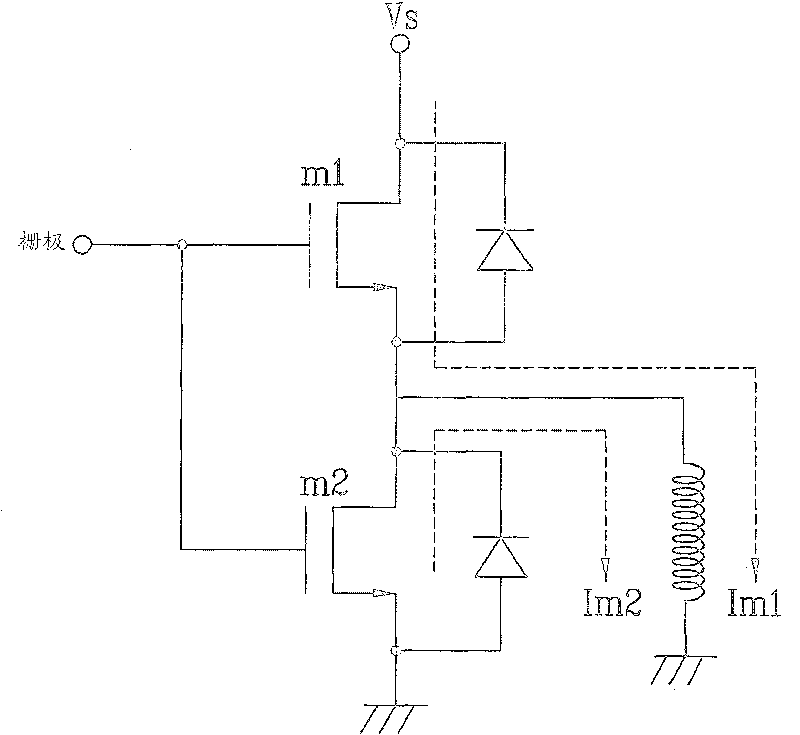
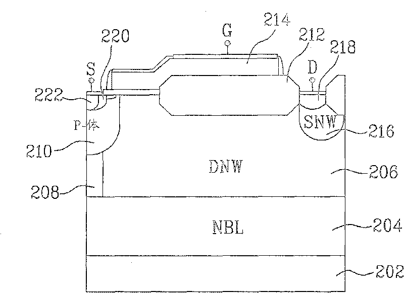
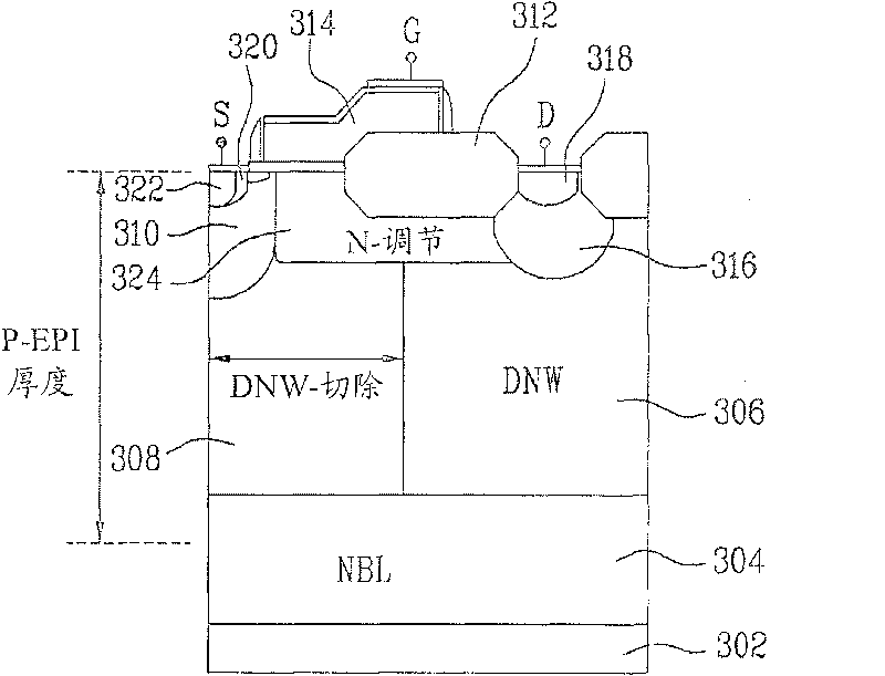
[0017] Reference will now be made in detail to the preferred embodiments of the invention, examples of which are illustrated in the accompanying drawings. Wherever possible, the same reference numbers will be used throughout the drawings to refer to the same or like elements.

[0018] as example Figure 3A As shown in , according to an embodiment, a high-side LDMOS may include: a P-type semiconductor substrate 302 having an N-type buried layer 304 formed thereon and / or thereover; and a P-type epitaxial layer having a thickness of P- epi. The N-type buried layer 304 can be used to reduce the width of the depletion layer extending from the P-type body 310 , so that when a voltage is applied to the N+-type drain region 318 , the breakdown voltage can be substantially increased. The P-type epitaxial layer can be used to reduce the impedance of the substrate 302 .

[0019] N-type deep well 306 may then be formed on and / or over P-type semiconductor substrate 302 . When implement...


PUM


Abstract

An LDMOS device and a method for fabricating the same that may include a first conductivity-type semiconductor substrate having an active area and a field area; a second conductivity-type deep well formed on the first conductivity-type semiconductor substrate; a second conductivity-type adjusting layer located in the second conductivity-type deep well; a first conductivity-type body formed in thesecond conductivity-type deep well; an insulating layer formed on the first conductivity-type semiconductor substrate in the active area and the field area; a gate area formed on the first conductivity-type semiconductor substrate in the active area; a second conductivity-type source area formed in the first conductivity-type body; a second conductivity-type drain area formed in the second conductivity-type deep well. Accordingly, such an LDMOS device has a high breakdown voltage without an increase in on-resistance.

Description

[0001] This application claims priority from Korean Patent Application No. 10-2007-0062849 (filed on June 26, 2007) based on 35 U.S.C §119, the entire contents of which are hereby incorporated by reference. technical field [0002] The present invention relates to a semiconductor device, and more particularly, to a lateral double diffused MOSFET (hereinafter, referred to as 'LDMOS') and a method of manufacturing the same. Background technique [0003] Bipolar-CMOS-DMOS (BCD) processing is a system-on-chip (SOC) technology that is widely used in automation applications, print head driving, monitoring, etc. LDMOS can be used as a main device in BCD processing and is mainly used in power integrated circuits (PICs). LDMOS devices have high input impedance compared to bipolar transistors, resulting in high power gain and simple gate drive circuitry. Furthermore, since the LDMOS device is a unipolar device, there is no time delay caused by storing or reorganizing minority carrier...

Claims


Application Information

Patent Timeline
Patent Type & Authority Patents(China)
IPC IPC(8): H01L21/336H01L29/78H01L29/06
CPCH01L29/66659H01L29/0878H01L29/66689H01L29/7816H01L29/086H01L29/42368H01L29/7835H01L29/1083H01L29/1079H01L29/0847H01L27/06
Inventor 高埑柱
Owner DONGBU HITEK CO LTD
Learn More