Semiconductor device with feedback control

a technology of feedback control and semiconductor devices, which is applied in semiconductor devices, amplifiers, amplifier modifications to extend bandwidth, etc., can solve the problems that the feedback from the output electrode to the input electrode can adversely affect the overall device and or circuit behavior, and the art electric field containment approaches do not deal with all of the feedback effects that can affect high frequency power devices

Active Publication Date: 2011-05-05
NXP USA INC
View PDF18 Cites 62 Cited by
  • Summary
  • Abstract
  • Description
  • Claims
  • Application Information

AI Technical Summary

Problems solved by technology

It is well known in electronic device, especially with transistors having very closely spaced electrodes, that feedback from the output electrodes to the input electrodes can adversely affect the overall device and or circuit behavior.
However, such prior art electric field containment approaches do not deal with all of the feedback effects that can afflict high frequency power devices.

Method used


Image

  • Semiconductor device with feedback control
  • Semiconductor device with feedback control
  • Semiconductor device with feedback control

Examples


case 1

Special ZT→∞. In this case the second term within the numerator parentheses vanishes, and in this limit

S12->2ZO(-jωMGD+1gm+jωCX)ΔS.Eq.21

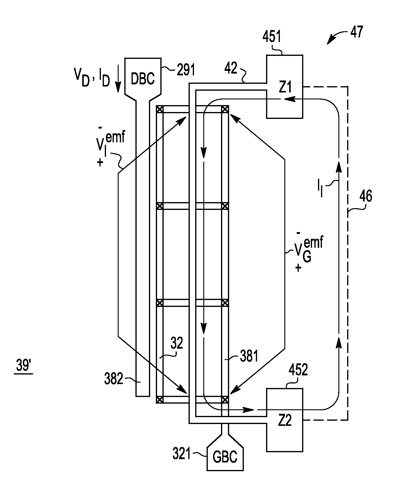
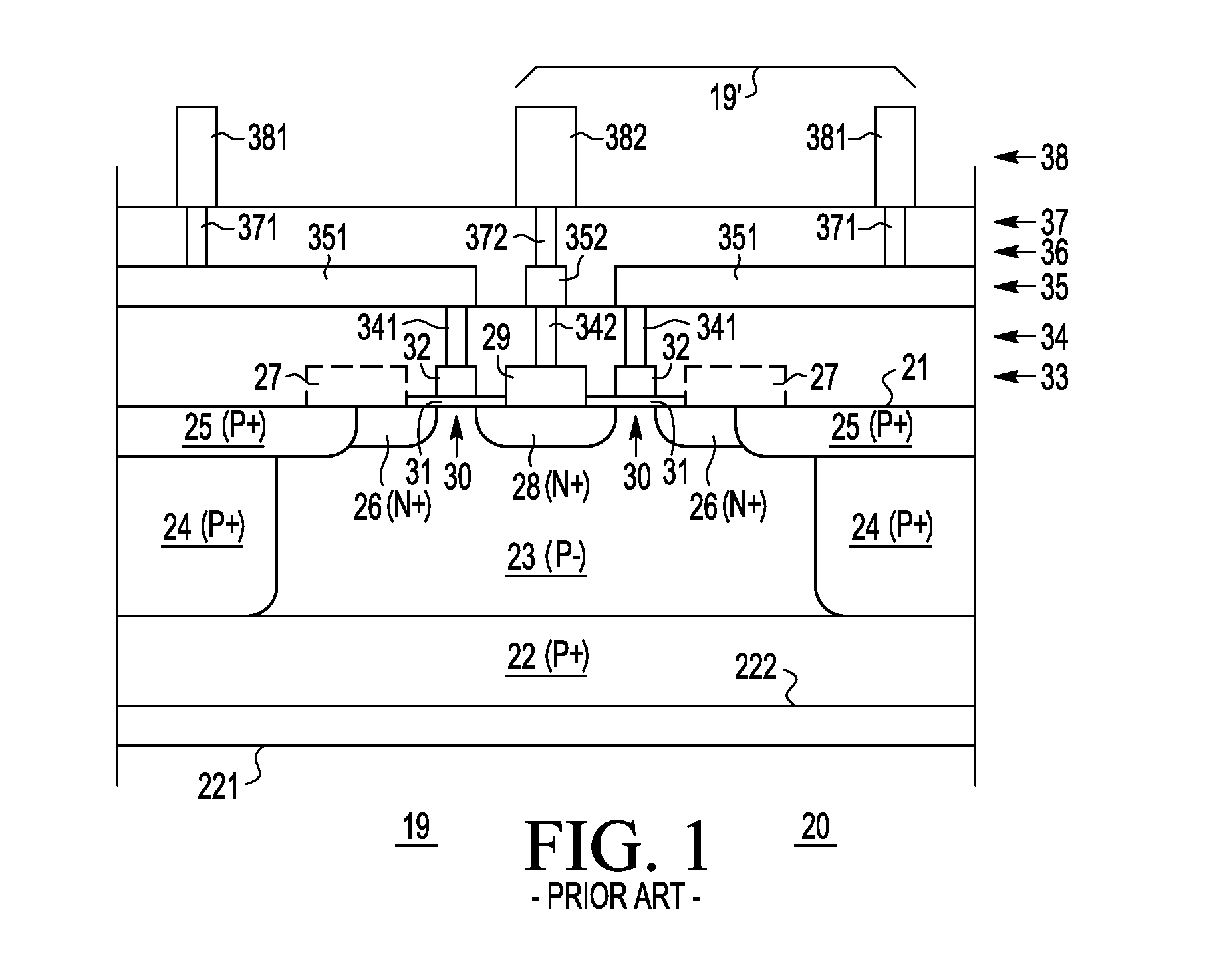
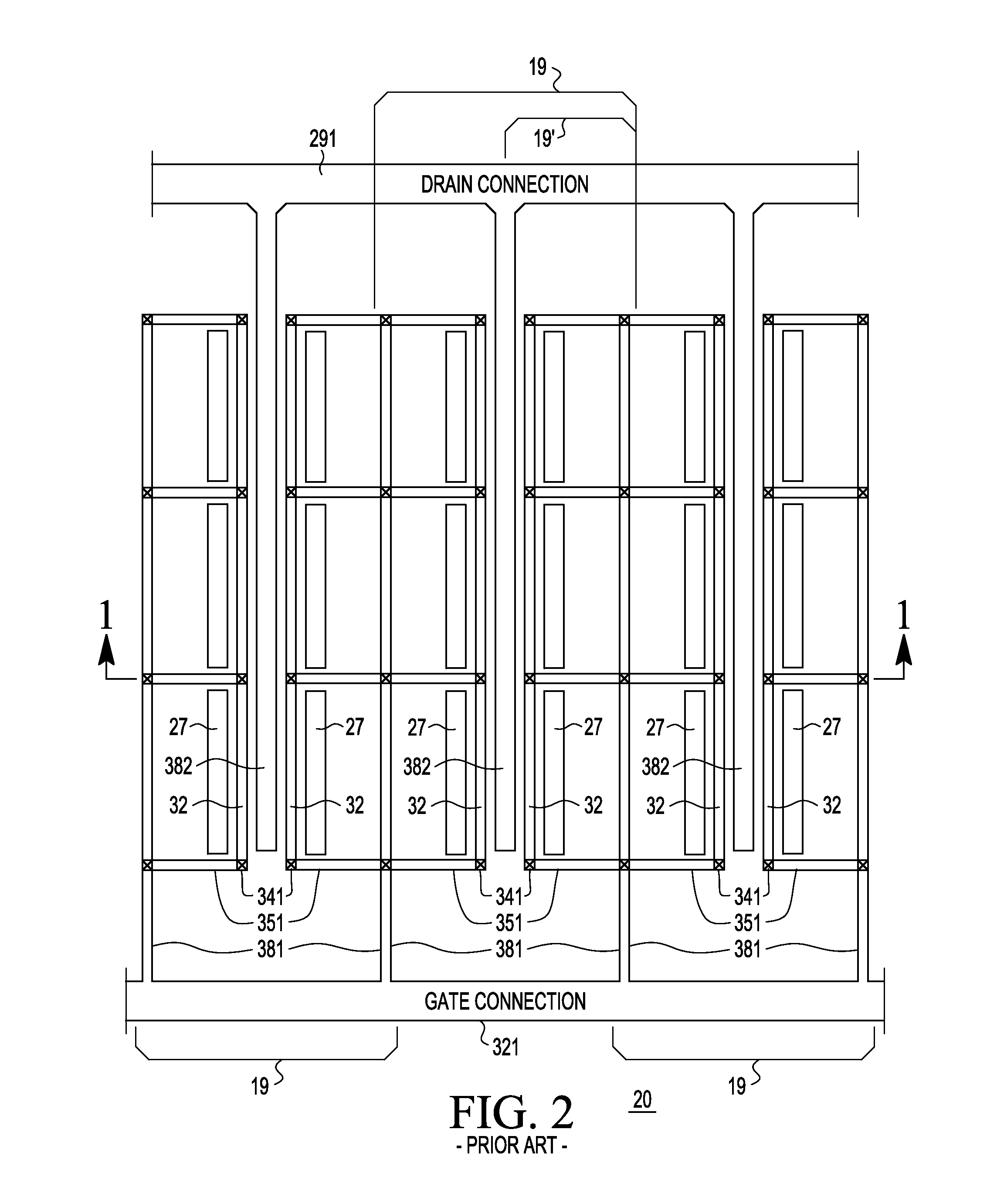
This corresponds to a standard LDMOS device without inductive interposer 42, that is, to portion 19′ of FIG. 3 and prior art device 19, 20 of FIGS. 1-2. The infinite impedance of ZT prevents any current flow in inductive interposer 42 and no inductive feedback compensation effect is present.

Special case 2: ZT=1 / (jωCT). In this case, ZT is in the form of, for example, an integrated capacitor of value CT chosen to resonate with the self inductance of inductive interposer 42. Substituting the expression for ZT into the equations for S12 makes the resonance explicit, and

S12=2ZO(-jωMGD-ω2MGIMIDRI+j(ωLI-1ωCT)+1gm+jωCX)ΔS.Eq.22

Special case 3: ZTRIT and RI have the effect of allowing large current flow in interposer 42, which current opposes the ordinary mutual inductance coupling between drain and gate and reduces the total effective drain-gate mutual ...

first embodiment

[0038] there is provided an electronic element (39′, 39, 40), comprising, an amplifying device having an input (32) with an input conductor (381) and an output (28, 29) with an output conductor (382), wherein the input (381) and output (382) conductors are substantially parallel for a first distance (391) and spaced apart by a second average distance (392), and an electrically conductive inductive interposer (42) forming part of a closed loop circuit (47), wherein the inductive interposer (42) is located between the output conductor (382) and the input conductor (381). According to a further embodiment, a ratio R of the first distance (391) divided by the second distance (392) has a value 1≦R≦100. According to a still further embodiment, R has a value 4≦R≦60. According to a yet further embodiment, the inductive interposer (42) is DC electrically isolated from the output conductor (382) and the input conductor (381). According to a yet still further embodiment, the inductive interpos...

second embodiment

[0039] there is provided a MOSFET device (39, 39′, 40) having a gate (32) and a drain (28), comprising, one or more input lead (381, 371, 351, 341) coupled to the gate (32), one or more output lead (382, 372, 352, 342, 29) coupled to the drain (28), wherein the one or more input lead (381, 371, 351, 341) and the one or more output lead (382, 372, 352, 342, 29) have portions (381, 382) that are spaced apart by at least a first distance (392) and substantially parallel along a second distance (391) larger than the first distance (392), and an electrically conductive interposer lead (42) adapted to be magnetically coupled when operating to the portions (381, 382) of the one or more input lead (381, 371, 351, 341) and the one or more output lead (382, 372, 352, 342, 29), the interposer lead (42) forming part of a closed loop circuit (47). According to a further embodiment, when operating a voltage induced on the portion (381) of the one or more input lead (381, 371, 351, 341, 32) by a c...


PUM


Abstract

An electronic element (39′, 39, 40) having feedback control is provided by placing an inductive interposer (42) between the output connection or bus (382) and the input connection or bus (381), wherein the inductive interposer (42) forms part of a closed circuit (47) with the inductive interposer (42) substantially parallel with the output connection or bus (382) and input connection or bus (381) for a distance permitting significant inductive coupling therebetween. In a preferred embodiment, the closed circuit (47) containing the inductive interposer (42) comprises impedance ZT. By including various circuit elements (e.g., resistance, capacitance, and / or inductance) in ZT, the output-to-input feedback can be modified to advantage. This greatly increases the available design freedom, especially for power devices, such as for example, field effect, MOSFET, LDMOS. bipolar and other power devices that use substantially parallel input and output bus structures.

Description

FIELD OF THE INVENTION[0001]The present invention generally relates to semiconductor (SC) devices and integrated circuits (ICs) and, more particularly, structures and methods for controlling output-to-input feedback in power devices and ICs.BACKGROUND OF THE INVENTION[0002]It is well known in electronic device, especially with transistors having very closely spaced electrodes, that feedback from the output electrodes to the input electrodes can adversely affect the overall device and or circuit behavior. In general, the severity of the problem increases with increasing frequency of operation because small parasitic elements, such as for example stray capacitance and mutual inductance, can have a greater effect as frequency increases. The effect of such stray capacitance with integrated circuits (ICs) and high frequency devices has been extensively studied and it is well known to attempt to ameliorate such adverse feedback by inserting a grounded metal shield between input and output...

Claims


Application Information

Patent Timeline
Patent Type & Authority Applications(United States)
IPC IPC(8): H03F1/00
CPCH01L23/4824H01L27/0207H01L27/0617H01L27/0688H01L2924/12044H01L2924/0002H01L2924/3011H01L2924/00H01L29/41758H01L29/78
Inventor LAMEY, DANIEL J.GUYONNET, MICHAEL
Owner NXP USA INC
Why Eureka
Try Eureka