Power LDMOS transistor

a technology of mos transistor and power ldmos, which is applied in the direction of basic electric elements, electrical equipment, semiconductor devices, etc., can solve the problem of inability to tightly control parameters, and achieve the effect of better control and reproducibility

Active Publication Date: 2007-02-15
CICLON SEMICON DEVICE
View PDF19 Cites 65 Cited by
  • Summary
  • Abstract
  • Description
  • Claims
  • Application Information

AI Technical Summary

Benefits of technology

[0009] The buffer layer serves to suppress the well documented short channel effects by helping to ensure that the depletion region does not reach too far into the channel. The buffer layer also provides a means for a better control and reproducibility of the breakdown voltage of the transistor. The breakdown is limited between the drain contact region and the buffer layer, rather than between the drain contact region and the upper surface of the substrate. In the prior art, the breakdown voltage is sensitive to the distance between the drain contact region and the diffusion profile of the dopant supplied by the substrate. In other words, the breakdown voltage in the prior art depends on the thickness of the epitaxial layer and on the doping concentration in the substrate which parameters can not be controlled tightly.

Problems solved by technology

In other words, the breakdown voltage in the prior art depends on the thickness of the epitaxial layer and on the doping concentration in the substrate which parameters can not be controlled tightly.

Method used


Image

  • Power LDMOS transistor
  • Power LDMOS transistor
  • Power LDMOS transistor

Examples


Embodiment Construction

[0017] As used herein, the following dopant concentrations are distinguished using the following notations: [0018] (a) N++ or P++: dopant concentration>5×10¹⁹ atoms / cm3; [0019] (b) N+ or P+: dopant concentration of 1×10¹⁸ to 5×10¹⁹ atoms / cm3; [0020] (c) N or P: dopant concentration of 5×10¹⁶ to 1×10¹⁸ atoms / cm3; [0021] (d) N— or P−: dopant concentration of 1×10¹⁵ to 5×10¹⁶ atoms / cm3; [0022] (e) N— or P−: dopant concentration 15 atoms / cm3.

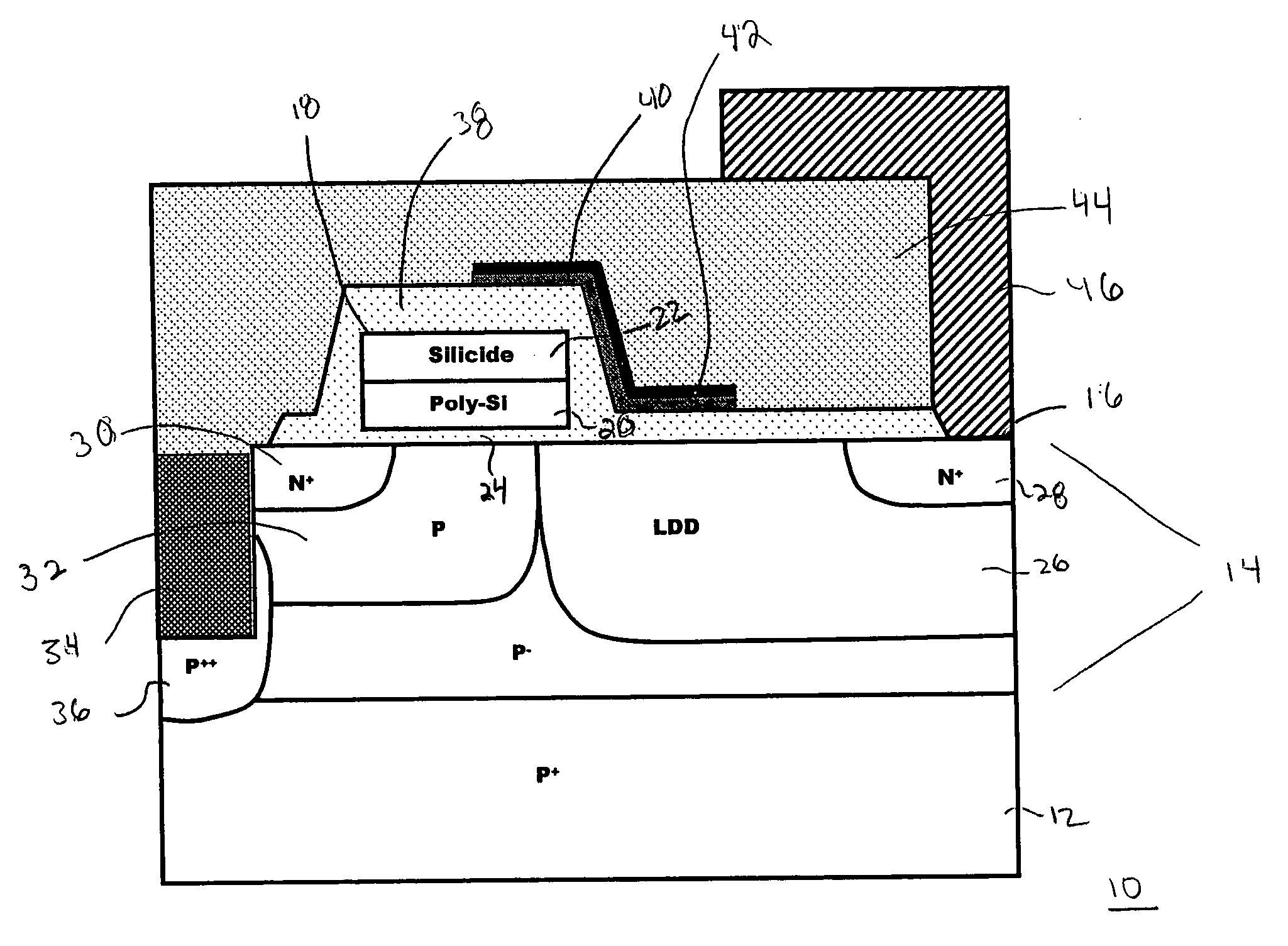
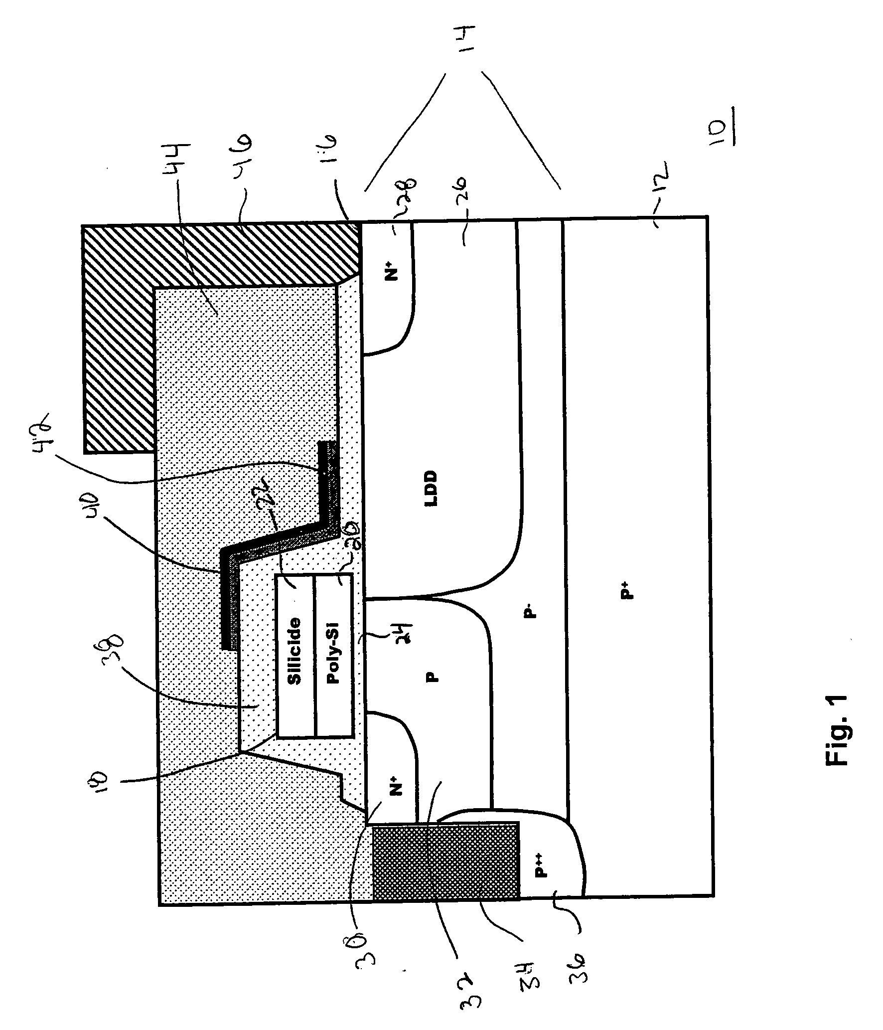
[0023]FIG. 1 is an illustration of a LDMOS transistor device 10, specifically an n-channel device. The transistor structure 10 illustrates different prior art transistor features, such as described in U.S. Pat. No. 6,831,332 to D'Anna et al., and in U.S. Pat. No. 5,252,848 to Adler et al., the entirety of which are hereby incorporated by reference herein and discussed later in more detail. The transistor structure 10 includes a semiconductor substrate 12, which, in the illustrated embodiment, is a highly doped (P+) silicon wafer doped with boron. A...


PUM


Abstract

A laterally diffused metal-oxide-semiconductor (LDMOS) transistor device includes a doped substrate having an epitaxial layer thereover having source and drain implant regions and body and lightly doped drain regions formed therein. The channel region and lightly doped drain regions are doped to a depth to abut the top surface of the substrate. In alternative embodiments, a buffer region of the second conductivity type and having dopant concentration greater than or equal to about the channel region is formed over the top surface of the substrate between the top surface of the substrate and the channel region and lightly doped drain region, wherein the channel region and lightly doped drain regions are doped to a depth to abut the buffer region.

Description

CROSS-REFERENCE TO RELATED APPLICATION [0001] This application is related to commonly assigned, co-pending U.S. patent application Ser. No. 11 / XXX,XXX, (Atty. Docket No. E3755-00006) of the same title, filed on the same date hereas, the entirety of which is hereby incorporated by reference herein.FIELD OF THE INVENTION [0002] The present invention relates to semiconductor structures and more particularly to laterally diffused MOS transistors (LDMOS), and still more particularly to LDMOS transistors designed for low voltage power management applications. BACKGROUND OF THE INVENTION [0003] Power MOSFETs (metal oxide semiconductor (MOS) field effect transistors (FET)) are used as electric switches for high frequency PWM (pulse width modulation) applications such as voltage regulators and / or as load switches in power applications. When used as load switches, where switching times are usually long, cost, size and on-resistance of the switches are the prevailing design considerations. Whe...

Claims


Application Information

Patent Timeline
Patent Type & Authority Applications(United States)
IPC IPC(8): H01L29/94H01L31/00H01L29/76
CPCH01L29/1083H01L29/1087H01L29/402H01L29/4175H01L29/7835H01L29/41775H01L29/456H01L29/4933H01L29/41766
Inventor XU, SHUMINGKOREC, JACEK
Owner CICLON SEMICON DEVICE
Why Eureka
Try Eureka