Isolated high-voltage LDMOS transistor having a split well structure

a transistor and split well technology, applied in the field of lateral power mosfet, can solve the problems of reliability problems, the electrical field maximum of the transistor occurs near the silicon surface, and the prior-art transistor is non-isolated source structur

Inactive Publication Date: 2005-06-07
FAIRCHILD TAIWAN
View PDF6 Cites 67 Cited by
  • Summary
  • Abstract
  • Description
  • Claims
  • Application Information

AI Technical Summary

Benefits of technology

[0009]The isolated high-voltage LDMOS transistor according to the present invention is manufactured on top of a P-substrate. A first diffusion region and a second diffusion region having N conductivity-type form an N-well disposed in the P-substrate. The first diffusion r

Problems solved by technology

One drawback of all of these prior arts is that the electric field maximum of the transistor occurs near the silicon surface.
This may cause reliability problems during high-temperature operation.
Another drawbac

Method used


Image

  • Isolated high-voltage LDMOS transistor having a split well structure
  • Isolated high-voltage LDMOS transistor having a split well structure
  • Isolated high-voltage LDMOS transistor having a split well structure

Examples


Embodiment Construction

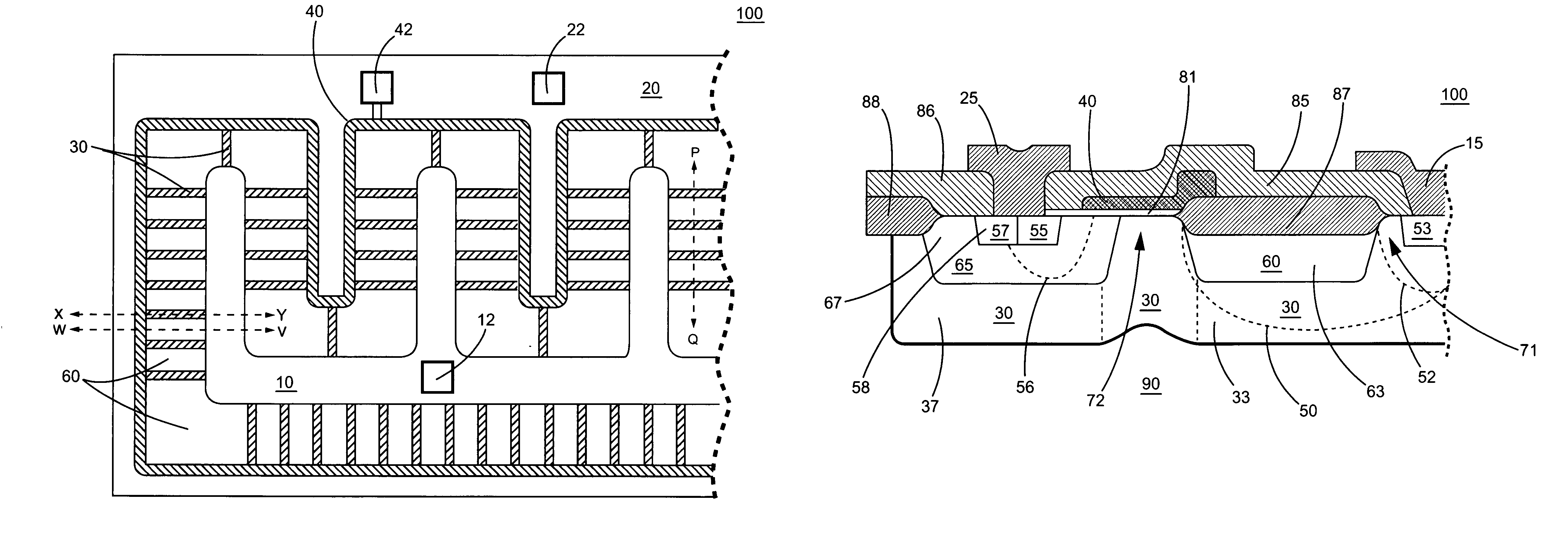
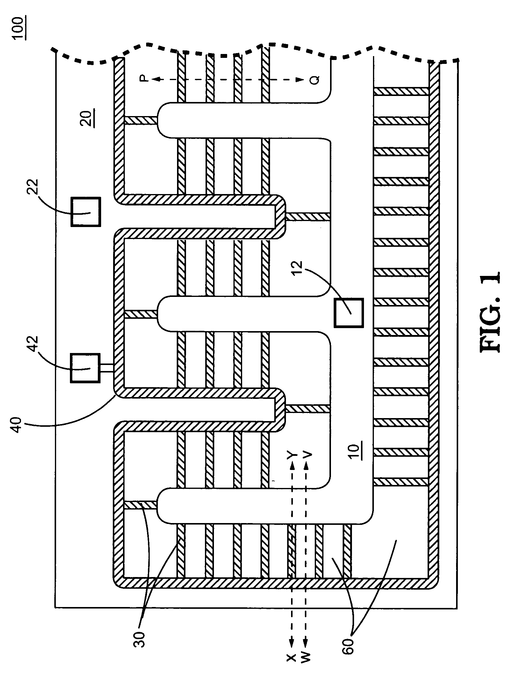
[0018]FIG. 1 is a top view of a LDMOS transistor 100 according to a preferred embodiment of the present invention. The LDMOS transistor 100 according to the present invention consists of a split N-well 30 and a P-well 60.

[0019]The LDMOS transistor 100 further includes a drain electrode 10, a source electrode 20, a polysilicon gate electrode 40, a bonding pad 12 for the drain electrode 10, a bonding pad 22 for the source electrode 20, and a bonding pad 42 for the polysilicon gate electrode 40. The P-well 60 splits the N-well 30. The N-well 30 is established from the drain electrode 10 to the source electrode 20.

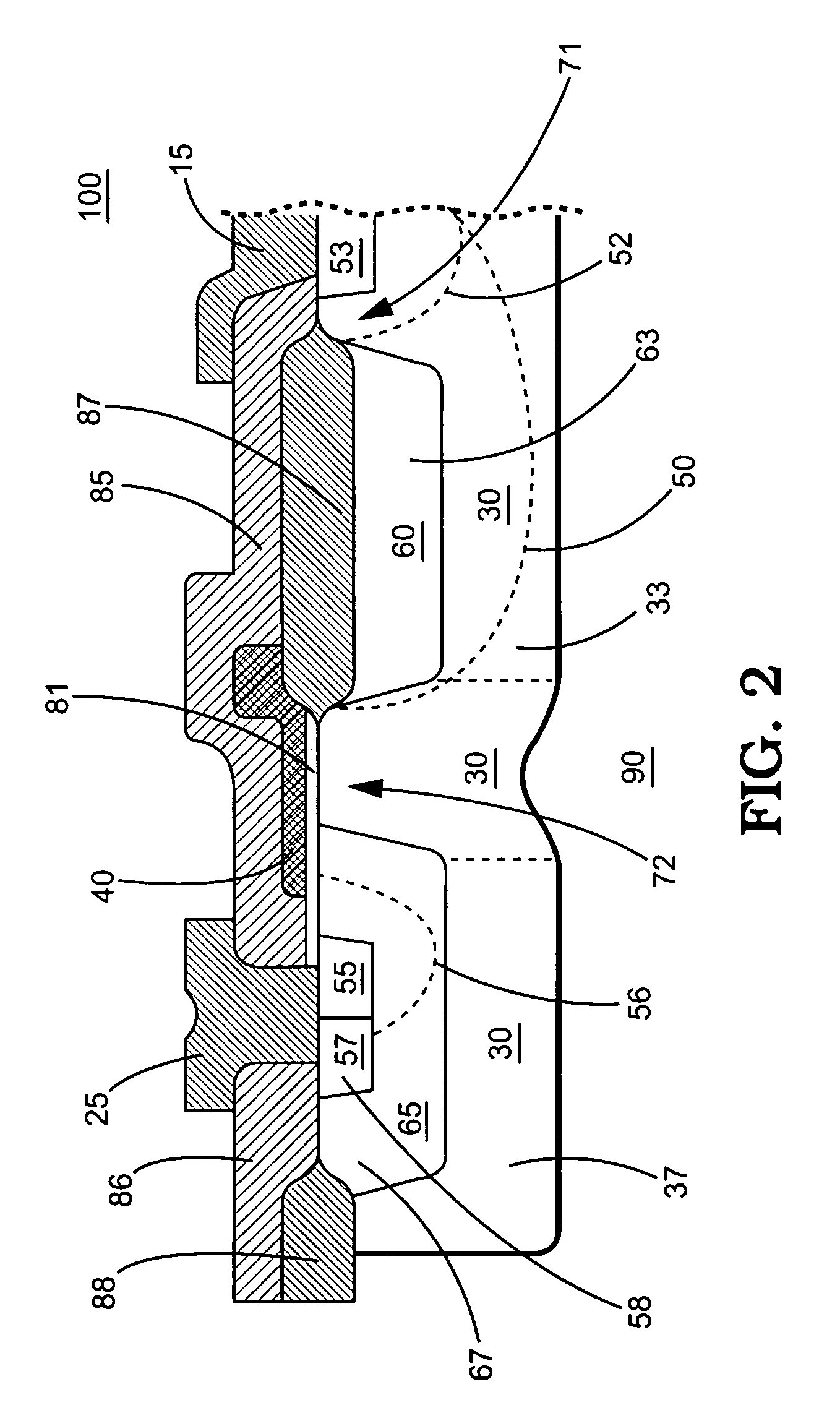
[0020]FIG. 2 is a first cross-sectional view of the LDMOS transistor 100 according to a preferred embodiment of the present invention. The LDMOS transistor 100 is shown between the source electrode 20 and the drain electrode 10. The first cross-sectional structure runs along the dotted line W-V in FIG. 1. FIG. 3 is a second cross-sectional view. The second cross-sectional stru...


PUM


Abstract

The isolated high-voltage LDMOS transistor according to the present invention includes a split N-well and P-well in the extended drain region. The P-well is split in the extended drain region of the N-well to form a split junction-field in the N-well. The split N-well and P-well deplete the drift region, which shifts the electric field maximum into the bulk of the N-well. This achieves a higher breakdown voltage and allows the N-well to have a higher doping density. Furthermore, the LDMOS transistor according to the present invention includes a N-well embedded beneath the source diffusion region. This creates a low-impedance path for the source region, which restricts the transistor current flow between the drain region and the source region.

Description

BACKGROUND OF THE INVENTION[0001]1. Field of the Invention[0002]The present invention relates to semiconductor devices, and more particularly to a lateral power MOSFET.[0003]2. Description of Prior Art[0004]The development of single chip processes for integrating power switches with control circuitry is a major trend in the field of power IC development. The LDMOS (lateral double diffusion MOS) process in particular is currently being applied to manufacture monolithic ICs. The LDMOS process involves performing planar diffusion on the surface of a semiconductor substrate to form a main current path oriented in the lateral direction. Since the lateral MOSFET is manufactured using a typical IC process, the control circuit and the lateral power MOSFET can be integrated onto a monolithic power IC. An LDMOS process using a reduced surface electric field (RESURF) technique with a low thickness EPI or N-well can achieve a high voltage with low on-resistance.[0005]Recently, many LDMOS design...

Claims


Application Information

Patent Timeline
IPC IPC(8): H01L29/76H01L23/58H01L29/78H01L23/62H01L29/66H01L27/085H01L27/088H01L29/94H01L29/06H01L29/08
CPCH01L29/0634H01L29/7816H01L29/0696H01L29/0886H01L29/42368H01L2924/0002H01L2924/00
Inventor HUANG, CHIH-FENGYANG, TA-YUNGLIN, JENN-YU G.CHIEN, TUO-HSIN
Owner FAIRCHILD TAIWAN
Why Eureka
Try Eureka