Inverted-trench grounded-source FET structure with trenched source body short electrode

a technology of inverted-trench grounded source and short electrode, which is applied in the direction of diodes, semiconductor devices, electrical apparatus, etc., can solve the problems of low manufacturing cost and achieve the effects of low manufacturing cost, reduced cell pitch and low manufacturing cos

Active Publication Date: 2008-03-20
ALPHA & OMEGA SEMICON LTD
View PDF1 Cites 68 Cited by
  • Summary
  • Abstract
  • Description
  • Claims
  • Application Information

AI Technical Summary

Benefits of technology

[0008]It is therefore an aspect of the present invention to provide a new and improved inverted ground-source trenched FET on highly doped substrate, e.g., highly doped N+ substrate, with a bottom-source and top-drain having a reduced cell pitch by using a trench body/source short structure without a P+ sinker thus achieving low manufacturi

Problems solved by technology

The low manufacturing cost is achieved because a low effective die cost wit

Method used


Image

  • Inverted-trench grounded-source FET structure with trenched source body short electrode
  • Inverted-trench grounded-source FET structure with trenched source body short electrode
  • Inverted-trench grounded-source FET structure with trenched source body short electrode

Examples


Embodiment Construction

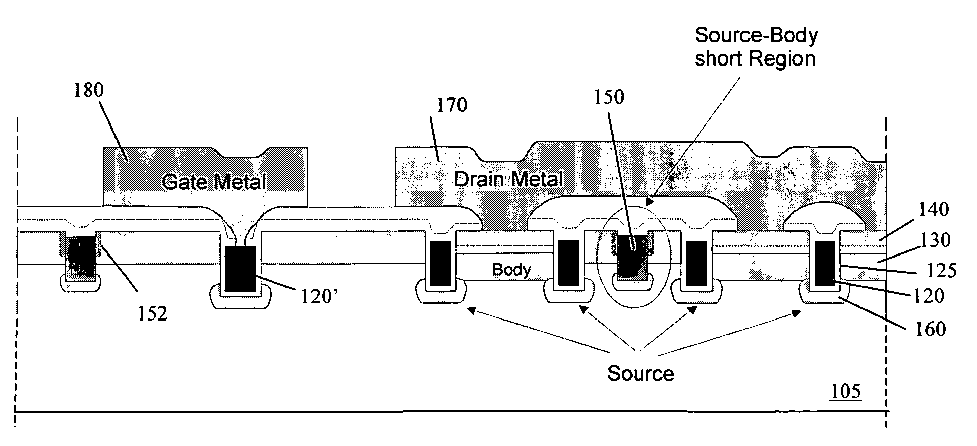
[0024]Referring to FIG. 2 for a cross sectional view of an inverted ground-source trenched FET device with a bottom source and a top drain of this invention. The inverted ground-source trenched FET device is supported on a N+ substrate 105 functioning as a bottom source electrode. A layer of P− epitaxial layer 110 functioning as a P-body region is supported on top of the substrate 105. The substrate is configured with an active cell area and a termination area typically disposed on the peripheral of the substrate. The FET device 100 has a plurality of trenches opened from the top surface of the substrate to reach to a lower portion of the epitaxial layer 110. The trenches opened in the active cell area is filled with gate polysilicon layer to form a gate 120 with the sidewalls of the trenches padded with a trench wall oxide layer 125. The trench in the termination area forms the gate runner 120′ with trenched gate 120 extended thereto. An N+ region 160 is disposed under the gate tre...


PUM


Abstract

This invention discloses bottom-source lateral diffusion MOS (BS-LDMOS) device. The device has a source region disposed laterally opposite a drain region near a top surface of a semiconductor substrate supporting a gate thereon between the source region and a drain region. The BS-LDMOS device further has a combined sinker-channel region disposed at a depth in the semiconductor substrate entirely below a body region disposed adjacent to the source region near the top surface wherein the combined sinker-channel region functioning as a buried source-body contact for electrically connecting the body region and the source region to a bottom of the substrate functioning as a source electrode. A drift region is disposed near the top surface under the gate and at a distance away from the source region and extending to and encompassing the drain region. The combined sinker-channel region extending below the drift region and the combined sinker-channel region that has a dopant-conductivity opposite to and compensating the drift region for reducing the source-drain capacitance.

Description

BACKGROUND OF THE INVENTION[0001]1. Field of the Invention[0002]The invention relates generally to the semiconductor power devices. More particularly, this invention relates to an inverted-trench grounded source field effect transistor (FET) structure that uses a conductive substrate with trench source body short electrode.[0003]2. Description of the Prior Art[0004]Conventional technologies to further reduce the source inductance for semiconductor MOSFET devices including the source inductance in FET; MOSFET and JFET devices are challenged by several technical difficulties and limitations. Specifically, there are technical challenges faced by those of ordinary skill in the art to reduce the source inductance. Meanwhile, there are ever increasing demand to reduce the source inductance in the semiconductor power devices because more and more power devices are required for applications that demand these devices to function with high efficiency, high gain, and high frequency. Generally,...

Claims


Application Information

Patent Timeline
IPC IPC(8): H01L29/78H01L21/336
CPCH01L21/823487H01L27/088H01L29/66734H01L29/7806H01L29/781H01L2924/0002H01L29/7811H01L2924/00
Inventor LUI, SIK KHEBERT, FRANCOISBHALLA, ANUP
Owner ALPHA & OMEGA SEMICON LTD
Why Eureka
Try Eureka