LDMOS device

a metal oxide semiconductor and transistor technology, applied in the direction of semiconductor devices, basic electric elements, electrical appliances, etc., can solve the problems of limiting the breakdown voltage capability of transistors and degrading rf performan

Inactive Publication Date: 2009-12-01
INFINEON TECH AG
View PDF12 Cites 60 Cited by
  • Summary
  • Abstract
  • Description
  • Claims
  • Application Information

AI Technical Summary

Problems solved by technology

High electric fields in these regions of an LDMOS transistor can cause punchthrough, avalanche breakdown, or other destructive effects, thus limiting the breakdown voltage capability of the transistor.
However, a lightly-doped drift region increases the on-state resistance of the LDMOS device which degrades RF performance.

Method used


Image

  • LDMOS device
  • LDMOS device
  • LDMOS device

Examples


Embodiment Construction

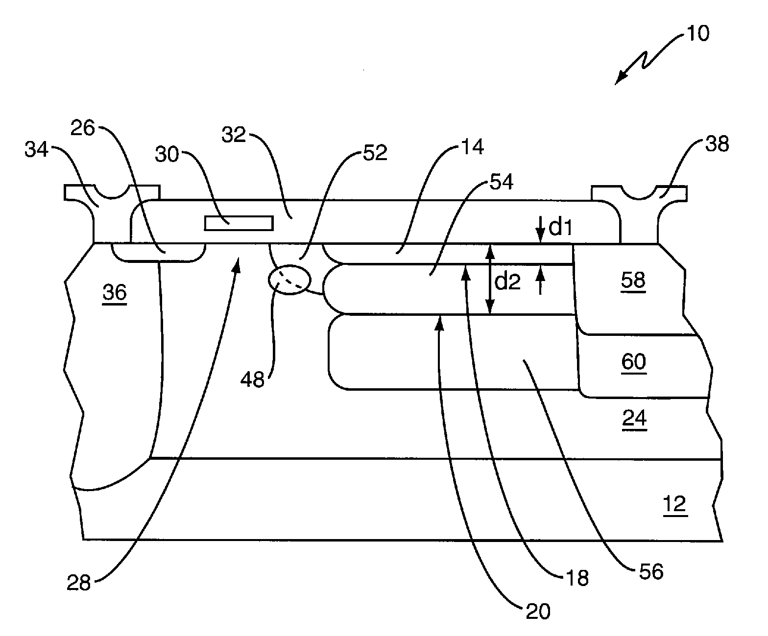
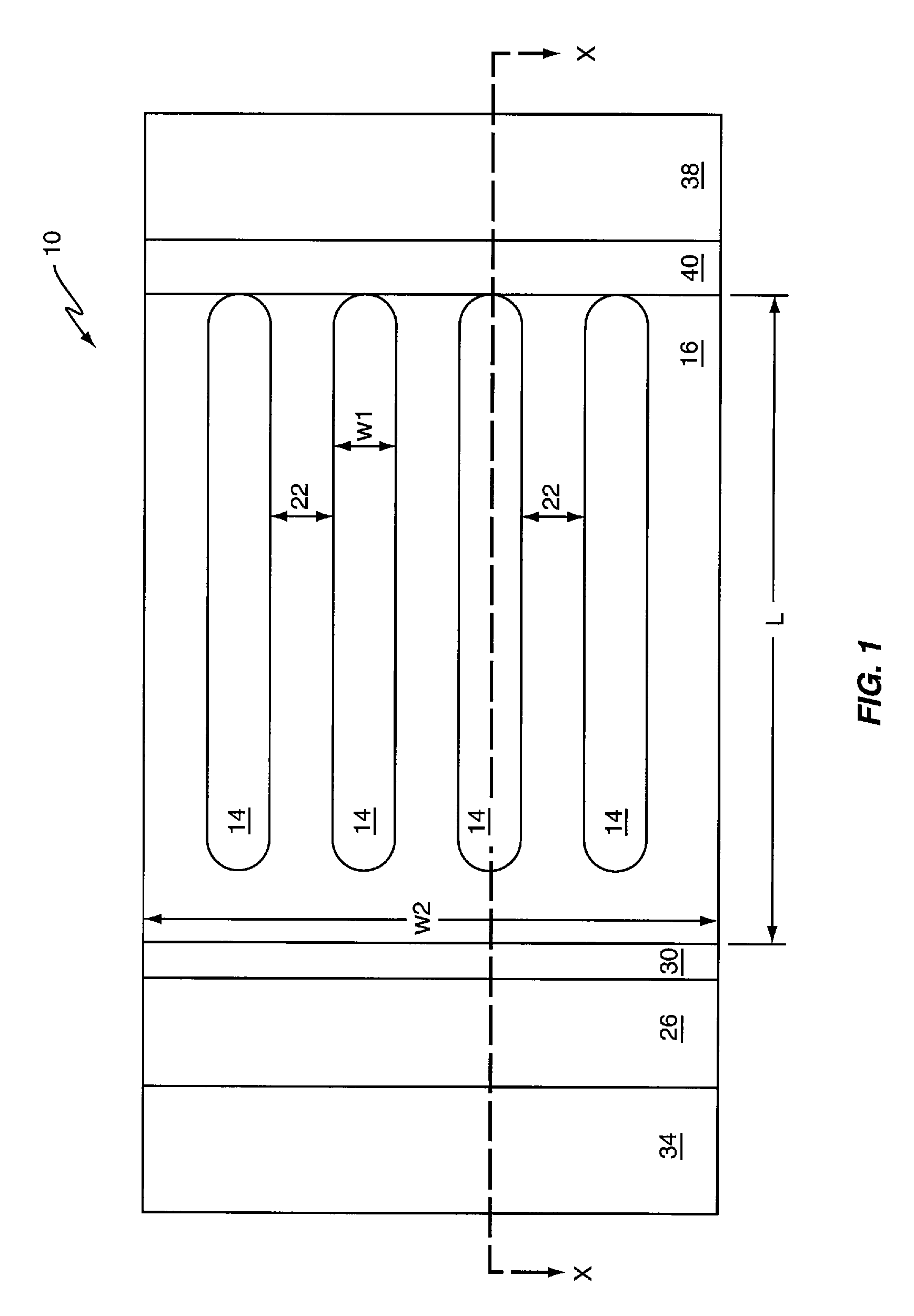
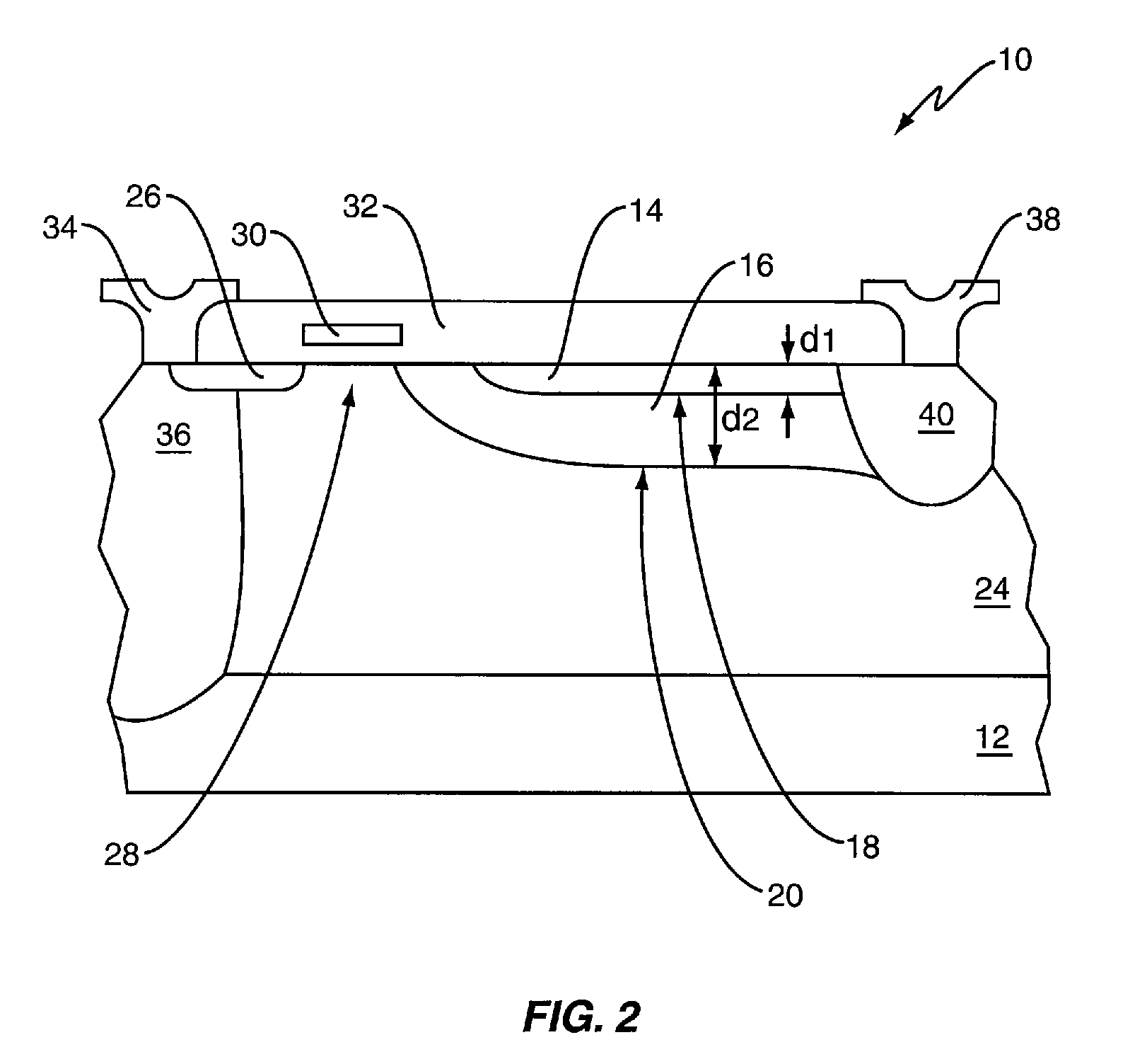
[0014]FIG. 1 illustrates a top-down view of one embodiment of a laterally diffused metal oxide semiconductor (LDMOS) transistor structure 10. FIG. 2 illustrates a cross-sectional view of the LDMOS transistor structure 10 along the line labeled ‘X’ in FIG. 1. The LDMOS transistor structure 10 is formed in a semiconductor substrate 12 such as a Si substrate and has a plurality of islands 14 disposed in an extended drain region 16 of the LDMOS transistor 10. The islands 14 are of the opposite conductivity type than the extended drain region 16, i.e., the extended drain region 16 has free negative charge carriers (n-type) while the islands 14 have free positive charge carriers (p-type). In other embodiments, the extended drain region 16 has free positive charge carriers (p-type) and the islands 14 have free negative charge carriers (n-type). The extended drain region 16, together with a drain contact region 40, surround each island 14, electrically isolating the islands 14 from each oth...


PUM


Abstract

An LDMOS transistor comprises source, channel and extended drain regions. The extended drain region comprises a plurality of islands that have a conductivity type that is opposite to the extended drain region. The islands have a depth less than a depth of the extended drain region.

Description

BACKGROUND OF THE INVENTION[0001]The present invention generally relates to laterally diffused metal oxide semiconductor (LDMOS) transistors, and particularly relates to LDMOS transistors having extended drain regions.[0002]LDMOS transistors are typically formed in an epitaxial layer deposited or grown on a semiconductor substrate. An LDMOS transistor has a source region separated from an extended drain region by a channel. The dopant distribution in the channel region is formed by lateral diffusion of dopants from the source side of the channel region, forming a laterally graded channel region. The source region and extended drain region are of the same conductivity type (e.g., n-type) while the epitaxial layer and the channel-region are of the opposite conductivity type (e.g., p-type). A gate actuates the LDMOS transistor. LDMOS transistors are used extensively in RF applications because of their advantageous linearity, power gain and breakdown voltage characteristics.[0003]The ex...

Claims


Application Information

Patent Timeline
Patent Type & Authority Patents(United States)
IPC IPC(8): H01L29/94H01L29/76
CPCH01L29/0634H01L29/7835H01L29/0696H01L29/1083H01L29/4175H01L29/0847
Inventor TORNBLAD, OLOFMA, GORDON
Owner INFINEON TECH AG
Why Eureka
Try Eureka