

Mask target and method for forming the same
A technology for aligning marks and grooves, applied to electrical components, electrical solid devices, circuits, etc., can solve the problems of difficult alignment and difficult acquisition of alignment signals, easy to achieve optical signals, and solve the problem of decreased or impossible alignment accuracy alignment effect
- Summary
- Abstract
- Description
- Claims
- Application Information
AI Technical Summary
Problems solved by technology
Method used
Image

Examples
Embodiment Construction
[0021] A new alignment mark of the contact window layer according to the present invention will be further described in detail below with reference to the accompanying drawings and specific embodiments.
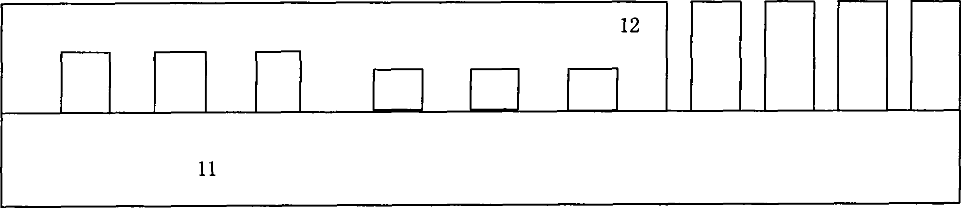
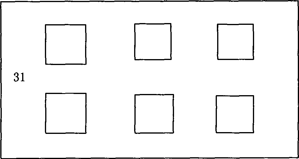
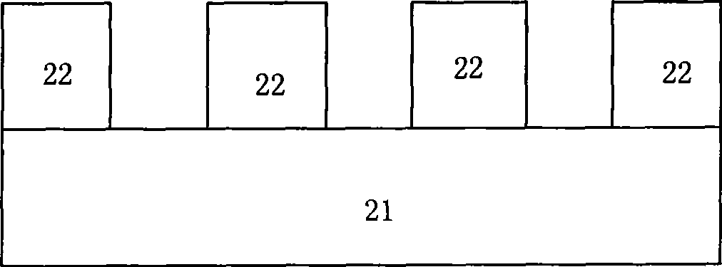
[0022] Figure 2A with 2B For the first step of the alignment mark in a preferred embodiment of the present invention, the field oxide layer 22 on the single crystal silicon substrate 21 is photolithographically or etched using the active layer mask 31, and the alignment mark is placed on the scribe line area begins to etch, forming a trench, shaped like Figure 2B As shown, in this embodiment, the thickness of the field oxide layer 22 is 1 μm. Of course, the thickness of the field oxide layer, the number and shape of trenches can be arbitrary, and are not limited by this embodiment.
[0023] Figure 3A with 3B For the second step of the alignment mark of a preferred embodiment of the present invention, first add a gate polysilicon layer 23 on the field oxide layer 22, an...
PUM
| Property | Measurement | Unit |
|---|---|---|
| thickness | aaaaa | aaaaa |
| thickness | aaaaa | aaaaa |
| thickness | aaaaa | aaaaa |
Abstract
Description
Claims
Application Information