Film processing device

A thin film processing and equipment technology, applied in the field of thin film processing equipment, can solve the problems of uneven deposition and etching films, degradation of film uniformity, etc.

Active Publication Date: 2009-05-27
JUSUNG ENG
View PDF1 Cites 1 Cited by
  • Summary
  • Abstract
  • Description
  • Claims
  • Application Information

AI Technical Summary

Problems solved by technology

Therefore, the deposited and etched thin film is not uniform ...

Method used


Image

  • Film processing device
  • Film processing device
  • Film processing device

Examples


Embodiment Construction

[0038] Reference will now be made in detail to the illustrated embodiments of the invention, which are illustrated in the accompanying drawings.

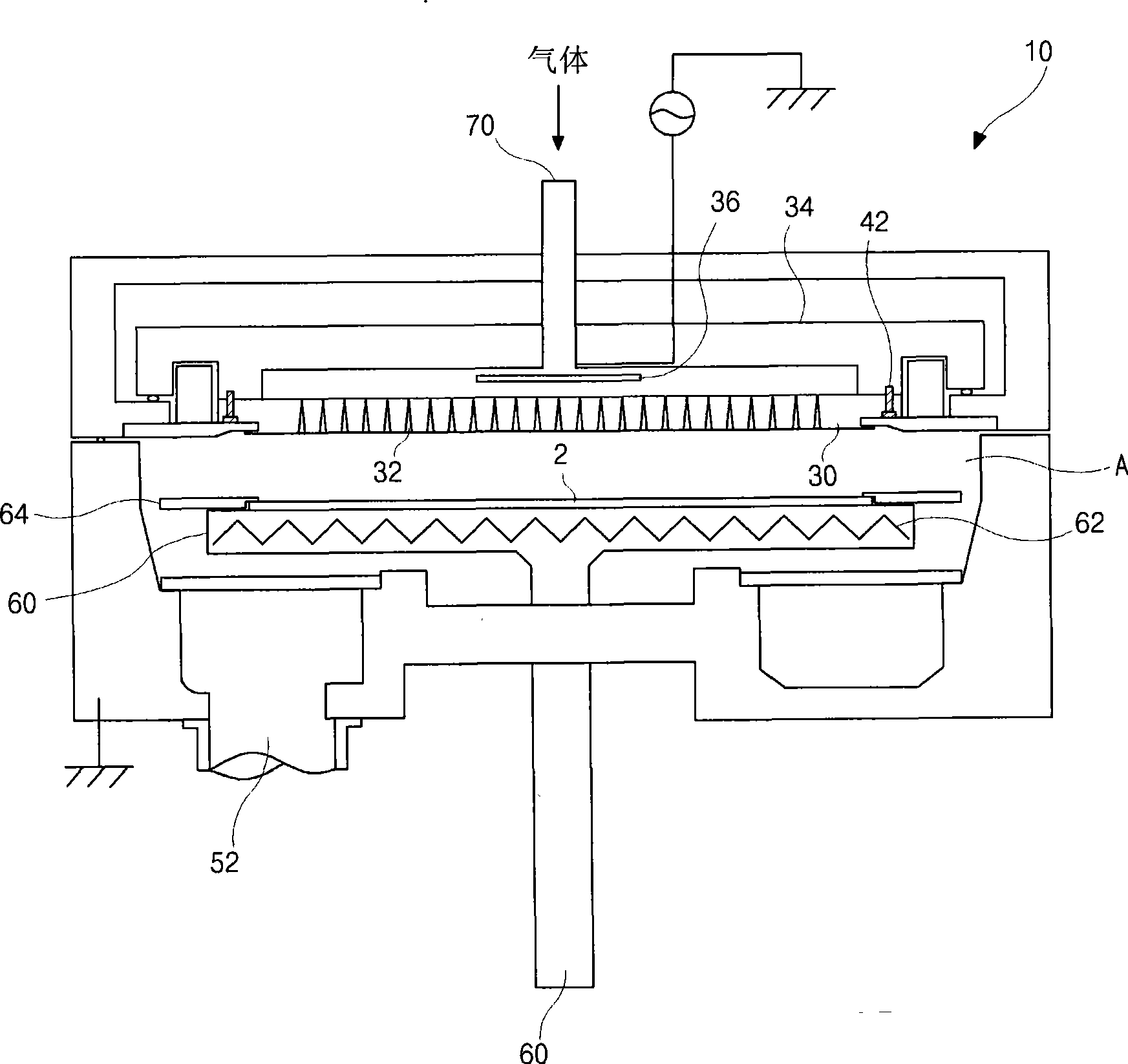
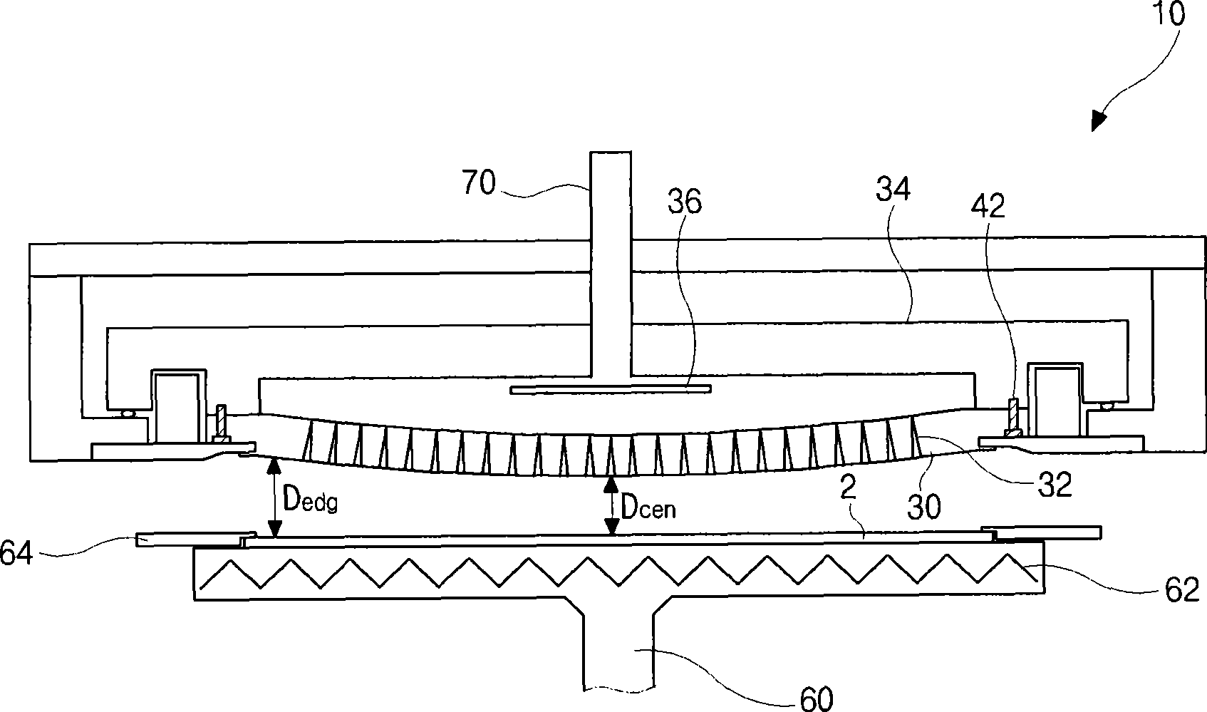
[0039] image 3 is a cross-sectional view illustrating a thin film processing apparatus according to a first embodiment of the present invention, and Figure 4 is to zoom in image 3 A view of area B.

[0040] see image 3 and 4 , the thin film processing apparatus according to the first embodiment includes a chamber 110 .

[0041] The reaction space A is in the processing chamber 110 and is a sealed space for performing a thin film processing process. The reaction space A is between the upper electrode 134 and the lower electrode 160 . The upper electrode 134 may be supplied with an RF high voltage, and the lower electrode 160 may be supplied with a bias voltage. The lower electrode 160 may serve as a chuck or a substrate replacement portion on which the substrate 102 is placed, and moves up and down.

[0042]Gas distributi...


PUM


Abstract

A film processing device including a chamber that includes a reaction space; an upper electrode which is in the chamber and includes plural through holes around the central part of the upper electrode; an air distribution plate, which is below the upper electrode and includes plural receiving holes corresponding to the plural through holes each; a coupling device, which passes through the throughholes and is inserted in the receiving holes to couple the upper electrode and the air distribution plate; a lower electrode, on which a substrate is arranged, and faces the air distribution plate, where the reaction space is between the lower electrode and the air distribution plate; a hermetic portion, which is on the surface of the top of the upper electrode around the through holes, where thehermetic portion is a O-shaped ring; and at least one refrigeration portion, which includes a refrigeration path so as to refrigerate the hermetic portion.

Description

[0001] This application claims the benefit of Korean Patent Application No. 10-2007-0118820 filed in Korea on Nov. 20, 2007, which is incorporated herein by reference. technical field [0002] The invention relates to a thin film processing device. Background technique [0003] Liquid crystal display devices, semiconductor devices (for example, solar cells), and the like are manufactured through various substrate-specific processes. For example, a thin film deposition process and a photolithography process and an etching process are performed several times to form a circuit pattern on the substrate, and additional processes such as a cleaning process, an attaching process, a cutting process, etc. are performed. [0004] The deposition process and the etching process are performed in chamber type thin film processing equipment. Recently, PECVD (Plasma Enhanced Chemical Vapor Deposition) equipment in which a reactive gas is excited in plasma using RF (Radio Frequency) high vo...

Claims


Application Information

Patent Timeline
IPC IPC(8): C23C16/513C23C16/04
CPCC23C16/45568C23C16/509C23C16/52
Inventor 车安基崔宰旭金东辉金友镇
Owner JUSUNG ENG
Why Eureka
Try Eureka