Electromagnetic bandgap structure and printed circuit board

An electromagnetic bandgap structure, printed circuit board technology, applied in the directions of printed circuit components, electrical connection printed components, circuits, etc., can solve problems such as incompatibility

Inactive Publication Date: 2009-06-10
SAMSUNG ELECTRO MECHANICS CO LTD
View PDF1 Cites 18 Cited by
  • Summary
  • Abstract
  • Description
  • Claims
  • Application Information

AI Technical Summary

Problems solved by technology

Especially when electronic equipment uses higher frequency bands, the typical bypass capacitor method or decoupling capacitor method used to solve the conduction noise problem is no longer suitable
[0013] Furthermore, when multiple active and passive devices need to be implemented in a c

Method used


Image

  • Electromagnetic bandgap structure and printed circuit board
  • Electromagnetic bandgap structure and printed circuit board
  • Electromagnetic bandgap structure and printed circuit board

Examples


Embodiment Construction

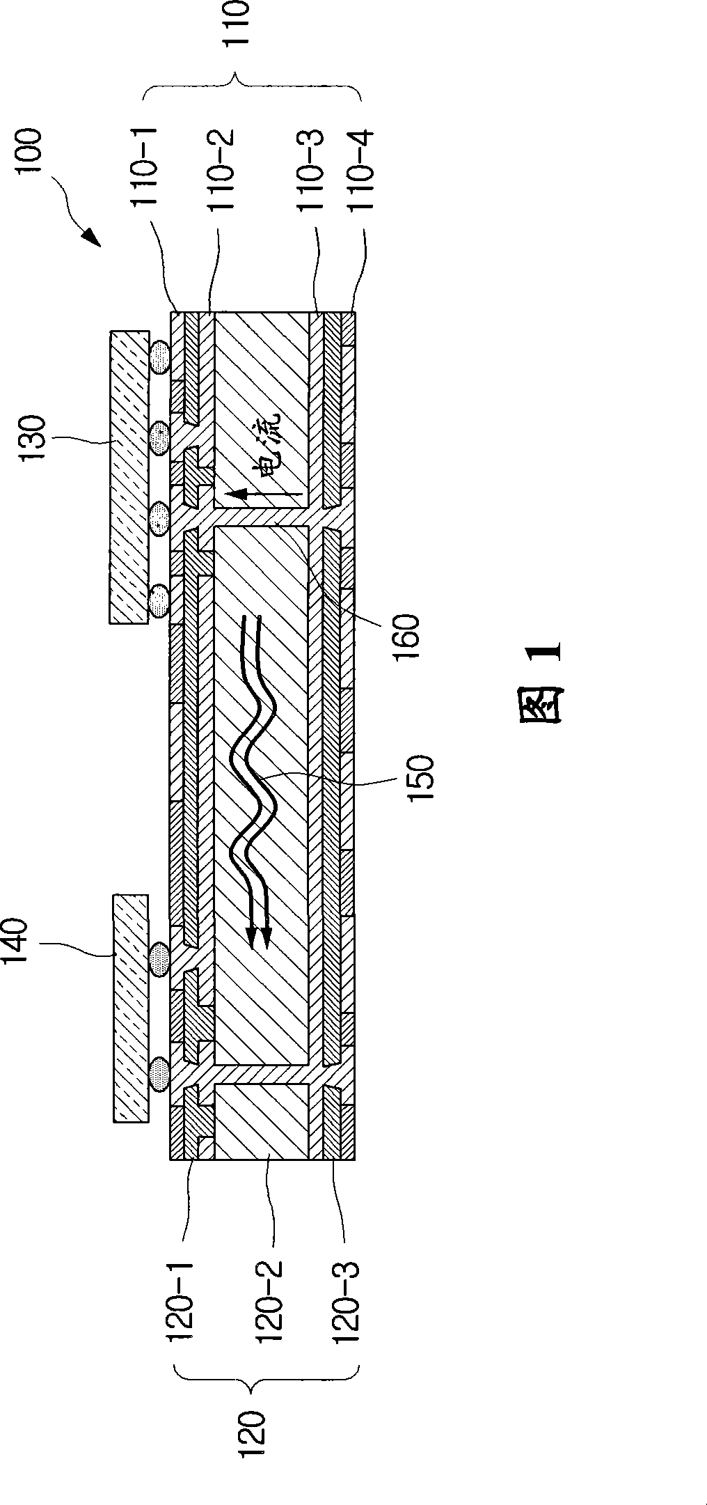
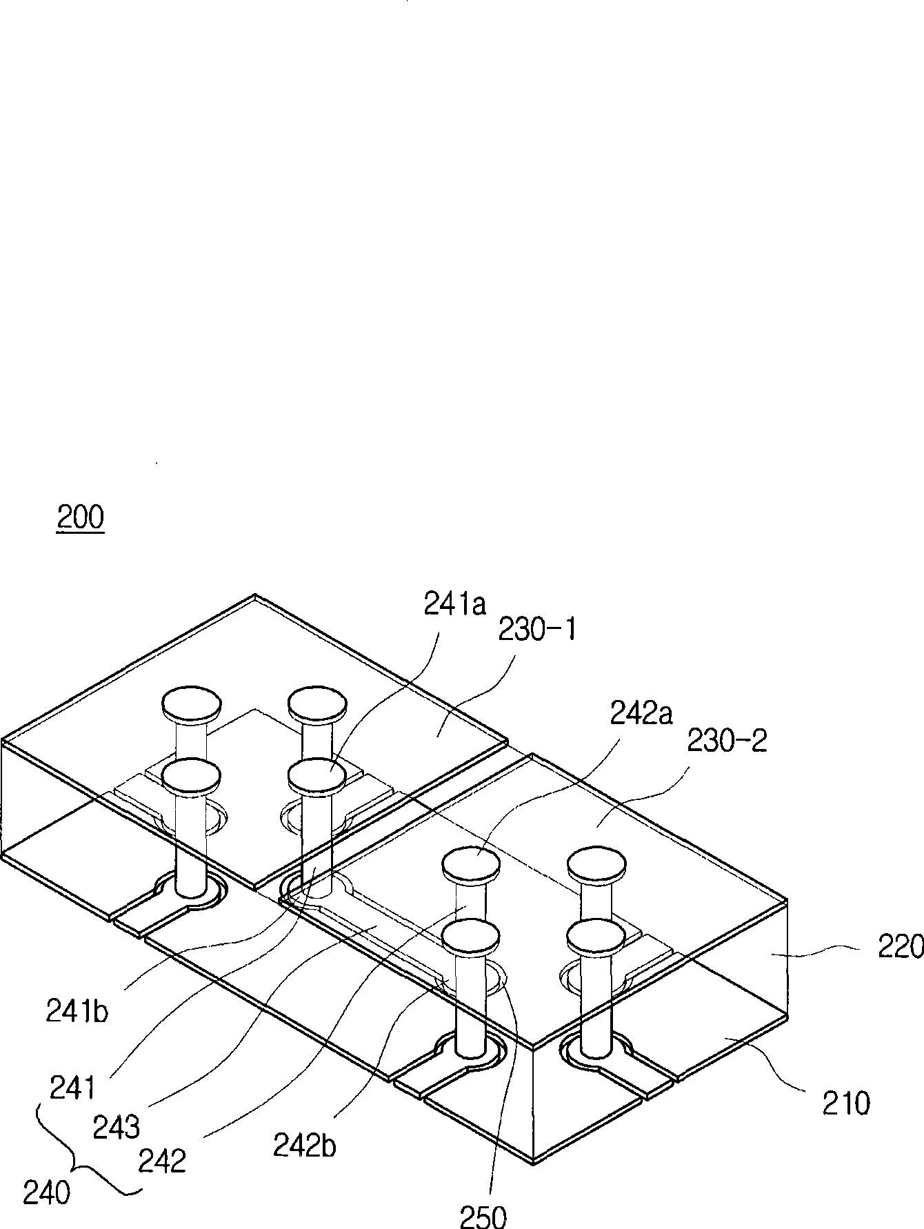
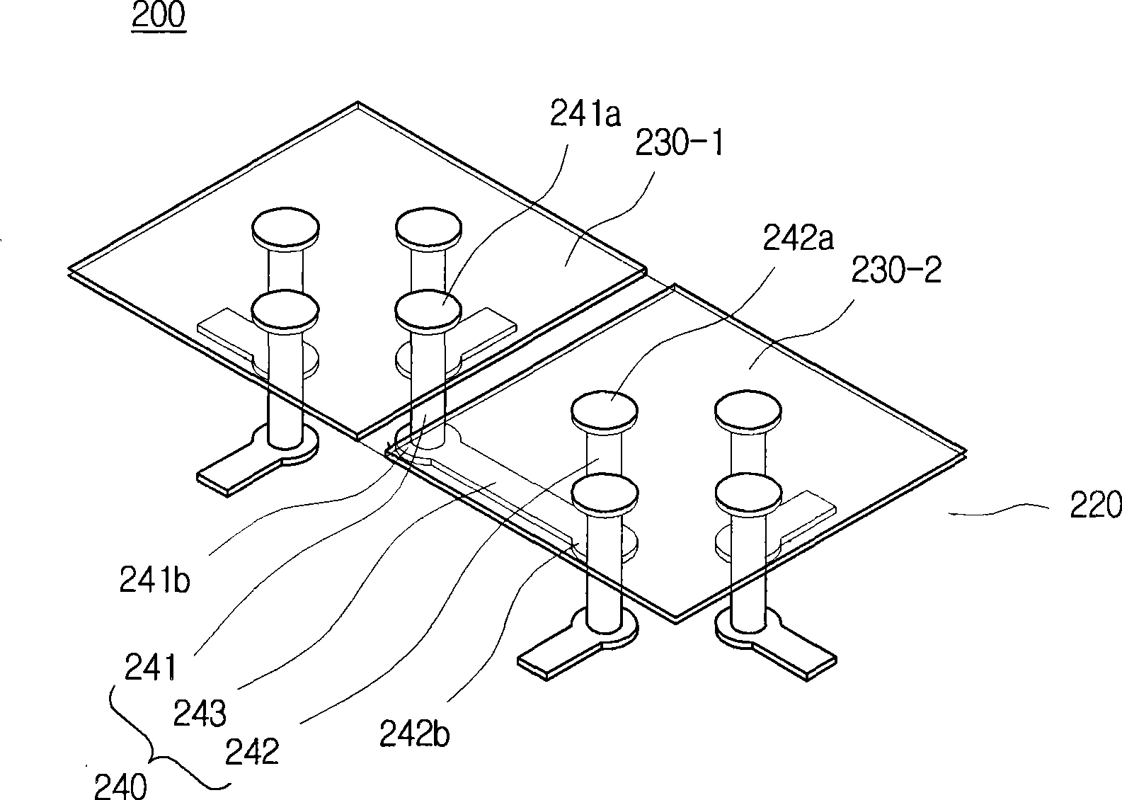
[0044] Since the invention is capable of many changes and embodiments, specific embodiments will be illustrated and described with reference to the accompanying drawings. However, this is not intended to limit the present invention to specific embodiments, but should be construed as including all changes, equivalents, and substitutions covered by the spirit and scope of the present invention. Throughout the figures, the same parts bear the same reference numerals. Throughout the description of the present invention, when it is determined that the description of a certain technique deviates from the point of the present invention, its related detailed description will be omitted.

[0045] Terms such as "first" and "second" may be used to describe various elements, but the above elements should not be limited to the above terms. The above terms are only used to distinguish one element from another. For example, a first element may be referred to as a second element and vice ve...


PUM


Abstract

The invention disclose an electromagnetic bandgap structure and printed circuit board euipped with the electromagnetic bandgap structure. According to the present invention, the board can include a dielectric layer; a plurality of conductive plates; and a stitching via, to electrically connect two of the conductive plates to each other. Here, the stitching via can include a first via and a second via, respectively, passing through the dielectric layer and having one end part being placed on a same planar surface as each of the two conductive plates; a connection pattern, having each end part being connected to the other end part of the first via and the second via, respectively; and a first extension pattern, placed on the same planar surface as one of the conductive plates and having one end part being connected to the one end part of the first via and the end part being connected to one of the conductive plates.

Description

[0001] Related Application Cross Reference [0002] This application claims priority from Korean Patent Applications No. 10-2007-0126760 and No. 10-2008-0057443 filed with the Korean Intellectual Property Office on December 7, 2007 and June 18, 2008, the disclosures of which are incorporated in their entirety This article is for reference only. technical field [0003] The present invention relates to an electromagnetic bandgap structure, and more particularly, to an electromagnetic bandgap structure capable of preventing signal transmission within a predetermined frequency band range and a printed circuit board having the electromagnetic bandgap structure. Background technique [0004] New electronic and communication devices are becoming increasingly smaller, thinner and lighter, reflecting today's emphasis on increased mobility. [0005] These electronic and communication devices have various complex electronic circuits (ie, analog circuits and digital circuits) for carr...

Claims


Application Information

Patent Timeline
IPC IPC(8): H05K1/02H05K1/11H01L23/498H01P3/08
CPCH01P1/2005H01L2224/16225H04B1/10H05K1/02H05K9/00
Inventor 韩美子朴大贤金汉
Owner SAMSUNG ELECTRO MECHANICS CO LTD
Why Eureka
Try Eureka