Electromagnetic bandgap structure and printed curcuit board

一种电磁带隙结构、印刷电路板的技术,应用在印刷电路、印刷电路、印刷电路零部件等方向,能够解决难以解决传导噪音、电子装置数字电路工作频率高、解决方法不适用等问题

Active Publication Date: 2009-02-11
SAMSUNG ELECTRO MECHANICS CO LTD
View PDF2 Cites 15 Cited by
  • Summary
  • Abstract
  • Description
  • Claims
  • Application Information

AI Technical Summary

Problems solved by technology

This has an adverse effect on the correct function / operation of the second circuit 140
[0012] Due to the increasing complexity of electronic devices and the higher operating frequency of digital circuits, it is becoming more and more difficult to solve this conducted noise problem
In particular, since electronic devices use higher frequency bands, the typical bypass capacitor method or decoupling capacitor method for solving the conduction noise problem is no longer applicable
[0013] Furthermore, when it is necessary to mount a plurality of active devices and passive devices on a complex wiring board (such as a system-in-package (Sip )) above, or when the operating frequency requires a high frequency band (such as in a network board), the previously mentioned solutions do not apply

Method used


Image

  • Electromagnetic bandgap structure and printed curcuit board
  • Electromagnetic bandgap structure and printed curcuit board
  • Electromagnetic bandgap structure and printed curcuit board

Examples


Embodiment Construction

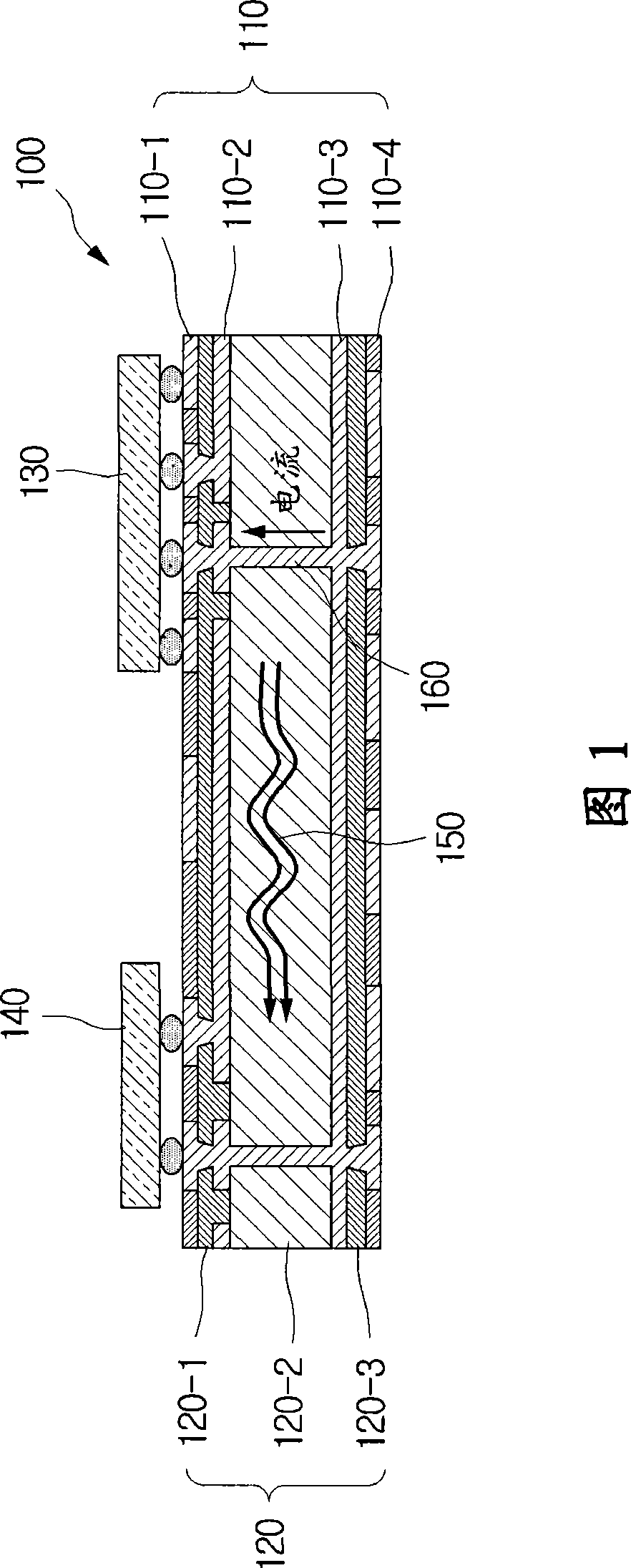
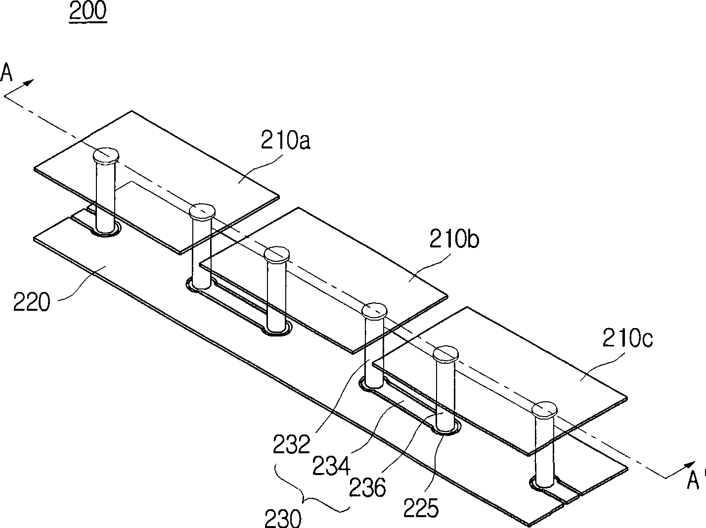
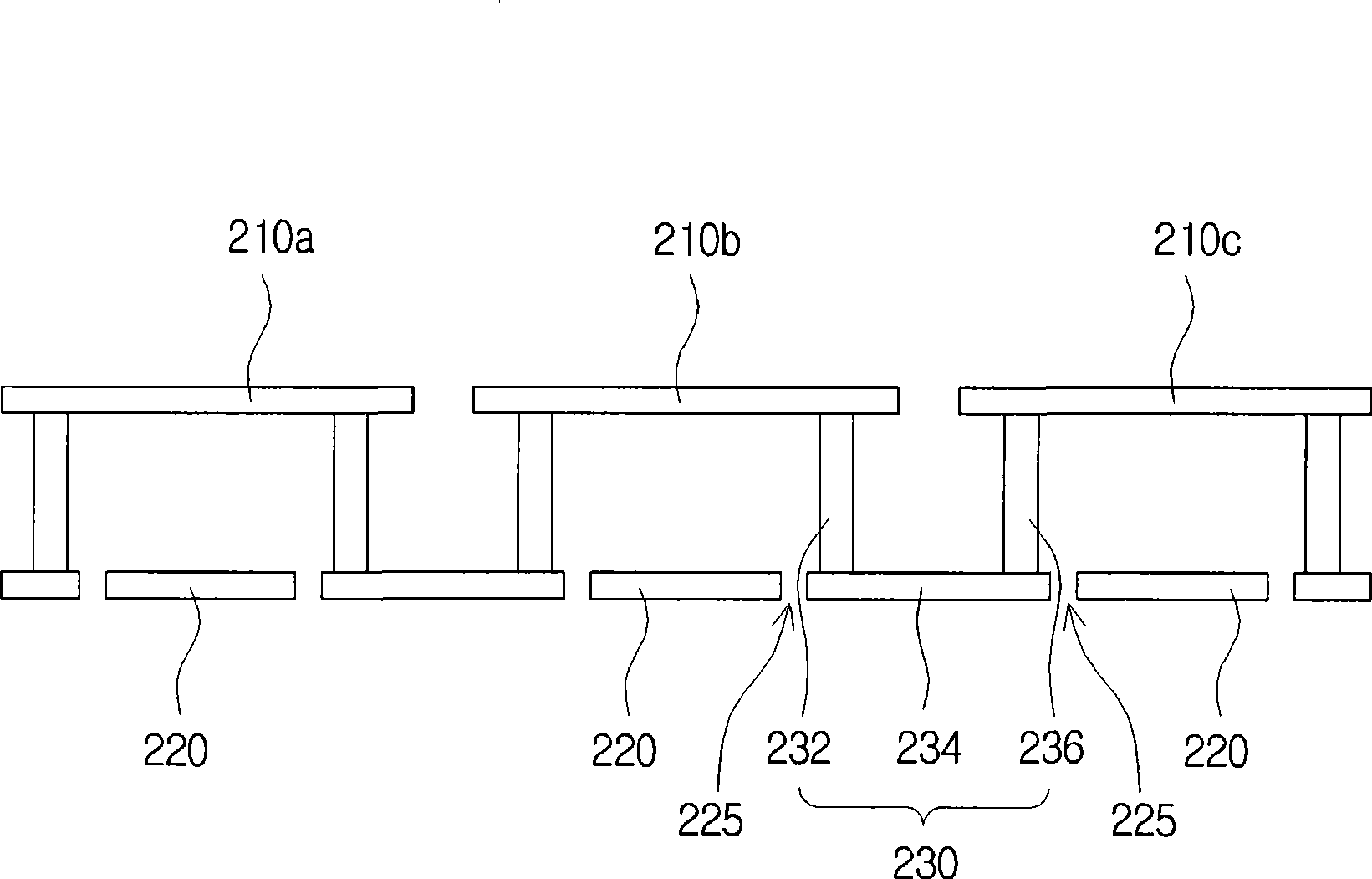
[0044] Since many variations and embodiments of the invention are possible, certain embodiments will be shown and described with reference to the drawings. However, the present invention is by no means limited to certain embodiments, but should be understood to include all modifications, equivalents, and replacements encompassed by the spirit and scope of the present invention. Like numbers refer to like elements throughout the drawings. Throughout the specification of the present invention, when describing a certain technique is considered not to relate to the gist of the present invention, the related detailed description will be omitted.

[0045] Terms such as 'first' and 'second' may be used in describing various elements, however, the above elements should not be limited to the above terms. The above terms are only used to distinguish one element from another. For example, a first element may be called a second element, and vice versa, without departing from the scope o...


PUM


Abstract

Disclosed are an electromagnetic bandgap structure and a printed circuit board including the same. In accordance with an embodiment of the present invention, the printed circuit board can include a dielectric layer, a plurality of conductive plates, and a stitching via, which is configured to electrically connect the conductive plates to each other. The stitching via can pass through the dielectric layer, and a part of the stitching via can be placed in a planar surface that is different from a planar surface in which the conductive plates are placed. With the present invention, the electromagnetic bandgap structure can prevent a signal of a predetermined frequency band from being transferred.

Description

[0001] Related Application Cross Reference [0002] This application claims the benefit of Korean Patent Applications No. 10-2007-0079261 and No. 10-2008-0057462 filed in the Korean Intellectual Property Office on Aug. 7, 2007 and Jun. 18, 2008, the disclosure of which is in its entirety incorporated herein by reference. technical field [0003] The present invention relates to an electromagnetic bandgap structure, and more particularly, to an electromagnetic bandgap structure which prevents transmission of signals varying within a predetermined frequency band and a printed circuit board having the electromagnetic bandgap structure . Background technique [0004] Reflecting today's emphasis on improved mobility, new electronic and communication devices are becoming smaller, thinner and lighter. [0005] These electronic and communication devices have various complex circuits (ie, analog circuits and digital circuits) to perform their functions and operations. Typically, t...

Claims


Application Information

Patent Timeline
Patent Type & Authority Applications(China)
IPC IPC(8): H05K1/02H05K1/11H01L23/498H01P3/08
CPCH05K2201/09309H01P1/2005H01Q15/0006H05K2201/09681H05K2201/09627H01Q15/006H05K1/0236H01L2224/16225H05K9/00H05K1/02H04B1/10
Inventor 金汉柳济光柳彰燮
Owner SAMSUNG ELECTRO MECHANICS CO LTD
Why Eureka
Try Eureka