Method for manufacturing hollowed-out board

A technology of hollowed-out boards and circuit boards, which is applied in the manufacture of printed circuits, printed circuits, electrical components, etc., and can solve problems such as poor punching deviation, uncertain distance between the punched opening 3' and the hollowed-out pattern 9, etc., so as to improve the punching accuracy and avoid Bad offset effect

Active Publication Date: 2009-06-10
靖江市城中村投资建设有限公司
View PDF0 Cites 6 Cited by
  • Summary
  • Abstract
  • Description
  • Claims
  • Application Information

AI Technical Summary

Problems solved by technology

[0003] However, the defect of this existing manufacturing method is that due to the influence of factors such as the lamination accuracy of the cover film, the lamination accuracy of the line film, and the lamination shrinkage difference of the cover film, the gap between the punched opening 3 ′ and the hollow figure 9 The distance between them is uncertain, so there is often a phenomenon of poor punching when stamping

Method used


Image

  • Method for manufacturing hollowed-out board
  • Method for manufacturing hollowed-out board
  • Method for manufacturing hollowed-out board

Examples


Embodiment Construction

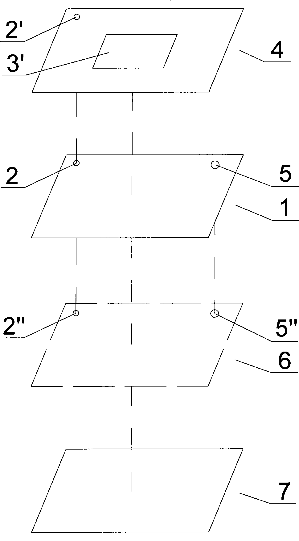
[0011] Below, combine image 3 with Figure 4 , the present invention is described in detail.

[0012] The method for manufacturing a hollow plate provided by the present invention includes: pressing the first covering film 14 formed with punching openings 13' and punching positioning holes 15' onto the first surface of the copper foil 11; After the circuit formation is completed on both sides, the second cover film 17 is pressed on the second surface of the copper foil 11 to obtain the circuit board 100; then punching is performed in alignment with the punching positioning hole 15' on the first cover film 14, Forming punching and positioning through-holes 18 on the circuit board 100; then punching the circuit board 100 based on the punching and positioning through-holes 18, so as to punch out hollow patterns 19 in the area of ​​the punching opening 13' .

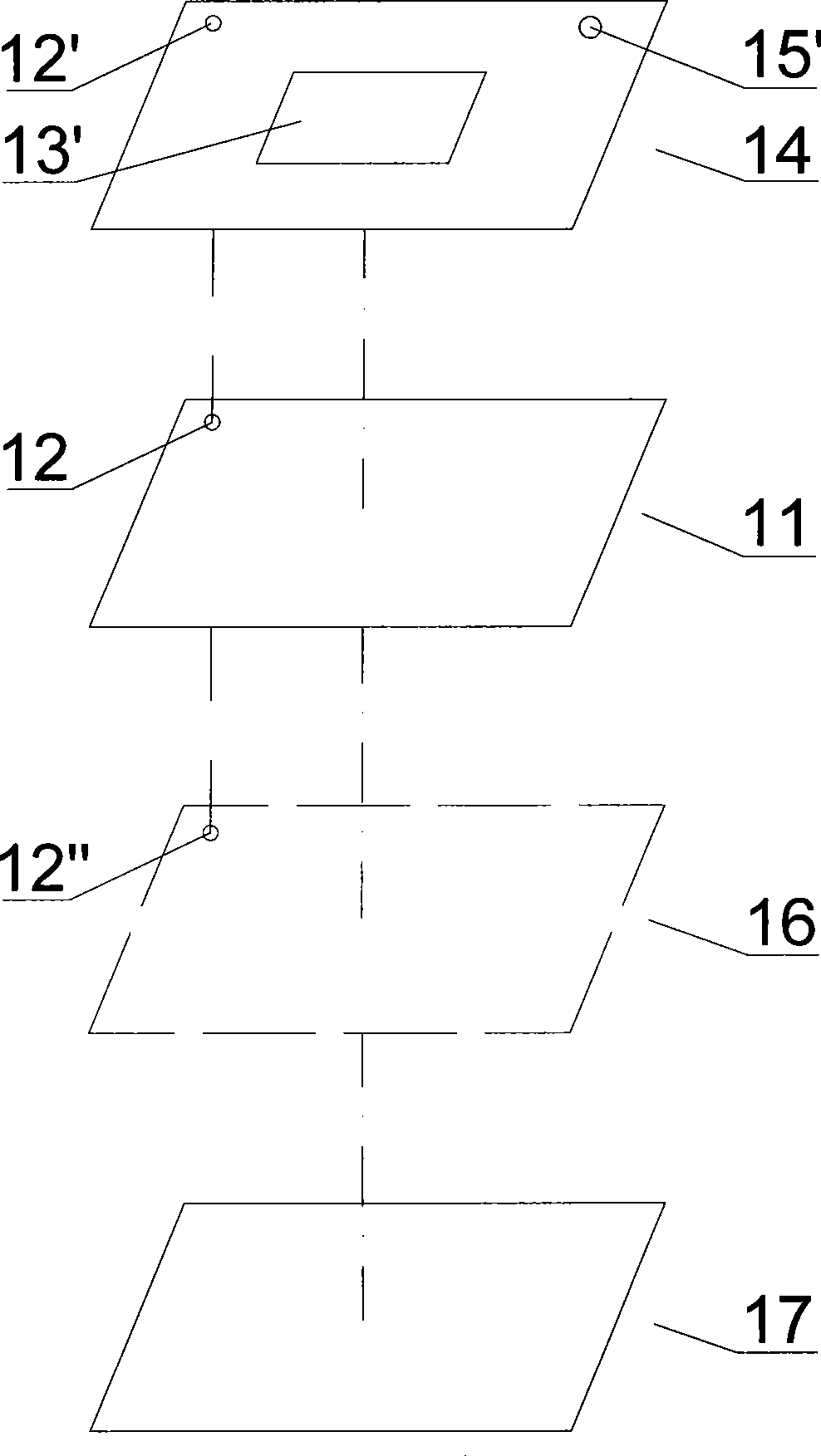
[0013] Preferably, a first press-fit alignment hole 12 is formed on the copper foil 11, a second press-fit alignment h...


PUM


Abstract

The present invention discloses a method for manufacturing a hollow board, which comprises the following steps: pressing a first covering film formed with a punching opening and a punching positioning hole on the first surface of a copper foil; then after a second surface of the copper foil is subjected to line molding, pressing a second covering film on the second surface of the copper foil so as to obtain a circuit board; subsequently, perforating in alignment with the punching positioning hole on the first covering film so as to form a punching positioning through hole on the circuit board; and then punching the circuit board taking the punching positioning through hole as a reference so as to punch out a hollow pattern within the area of the punching opening. The method for manufacturing the hollow board has the advantages that the distance between the punching opening and the punching positioning through hole is kept unchanged, so the distance between the punching opening and the hollow pattern is ensured to be unchanged, the punching precision is improved, and the phenomenon of poor deflective punching is avoided effectively.

Description

technical field [0001] The invention relates to the field of printed circuit board manufacturing, and more specifically, relates to a method for manufacturing a hollow board. Background technique [0002] Usually, the hollow board is one of the printed circuit boards, which is formed by laminating cover films on both sides of the copper foil, and punching out partial hollow patterns on the circuit board through a stamping process. Such as figure 1 As shown, the existing hollow board manufacturing process is generally as follows: firstly, the first press-fit alignment hole 2 is drilled on the copper foil 1; A cover film 4 is press-fitted on the first surface of the copper foil 1, and it is ensured that the second press-fit alignment hole 2' on the first cover film 4 is aligned with the first press-fit pair drilled on the copper foil 1. The position holes 2 are aligned; then the line film 6 formed with the third pressing alignment hole 2 "and the punching positioning hole 5"...

Claims


Application Information

Patent Timeline
IPC IPC(8): H05K3/00
Inventor 张超尤健
Owner 靖江市城中村投资建设有限公司
Why Eureka
Try Eureka