Phase change memory dynamic resistance test and manufacturing methods

A technology of phase change and storage unit, which is applied in the direction of static memory, digital memory information, information storage, etc., and can solve the problems of smaller active area and lower current value

Inactive Publication Date: 2009-10-21
MACRONIX INT CO LTD +1
View PDF11 Cites 9 Cited by
  • Summary
  • Abstract
  • Description
  • Claims
  • Application Information

AI Technical Summary

Problems solved by technology

Various implemented techniques hope to make this active area smaller, so that the current value that causes the phase change is reduced

Method used


Image

  • Phase change memory dynamic resistance test and manufacturing methods
  • Phase change memory dynamic resistance test and manufacturing methods
  • Phase change memory dynamic resistance test and manufacturing methods

Examples


Embodiment Construction

[0045] The features, objectives and advantages of the present invention can be fully understood through the following description of the attached drawings, embodiments and claims.

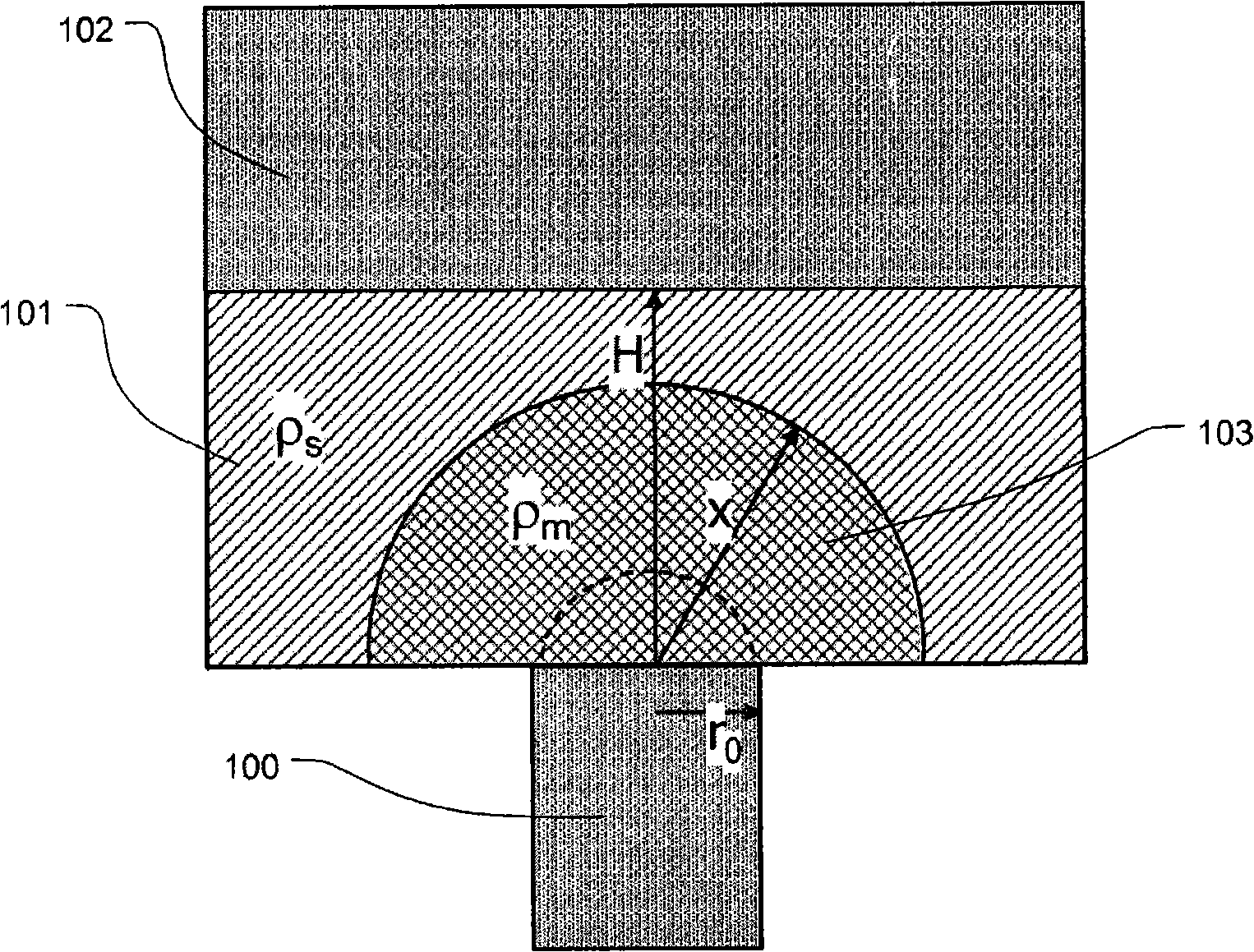
[0046] Subsequent descriptions of the invention will refer to Figure 1 to Figure 8 . figure 1 A simple diagram of a mushroom-shaped phase change memory cell comprising a bottom electrode 100 , comprising a phase change material element 101 , and a top electrode 102 . The bottom electrode 100 in the described embodiment is a 0 The columnar shape, and the interface between the phase change material element 101 and the bottom electrode 100 has a contact area of ​​about πr 0 2 . The area where the top electrode 102 is connected to the phase change material element 101 is substantially larger than the contact area between the bottom electrode 100 and the phase change material element 101 .

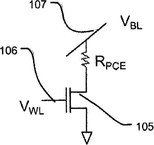
[0047] In operation, the bias circuit (for example see Figure 5 A bias circuit voltage and current source...


PUM


Abstract

A method for testing an integrated circuit memory device includes applying a sequence of test pulses to a memory cell on the device, where the test pulses result in current through the memory cell having an amplitude dependent on the test pulse. Resistance in the memory cell is measured in response to the sequence of test pulses. A parameter set is extracted from the resistance measurements which includes at least one numerical coefficient that models dependency of the measured resistance on the amplitude of the current through the memory cell. The extracted numerical coefficient or coefficients are associated with the memory device, and used for controlling manufacturing operations.

Description

technical field [0001] The present invention relates to high density memory devices using phase change memory materials, such as chalcogenides and other materials, and methods of making such devices. Background technique [0002] These phase change memory materials, such as chalcogenides and similar materials, can be caused to change crystal phase by applying a current of magnitude suitable for use in integrated circuits. Generally speaking, the characteristic of the amorphous state is that its resistance is higher than that of the crystalline state, and this resistance value can be easily measured and used as an indicator. This property has sparked interest in using programmable resistive materials to form non-volatile memory circuits that can be used for random access reading and writing. [0003] The transition from the amorphous state to the crystalline state is generally a low current step. The transition from the crystalline state to the amorphous state (hereinafter ...

Claims


Application Information

Patent Timeline
Patent Type & Authority Applications(China)
IPC IPC(8): G11C29/00
CPCG11C29/50008G11C29/50G11C13/0004Y10T29/49004
Inventor 李明修拉詹德瑞·毕平林仲汉
Owner MACRONIX INT CO LTD
Why Eureka
Try Eureka