Non-contact process kit

A kit and coupling technology, applied in the field of non-contact processing kits, can solve problems such as temperature changes of the shielding ring

Active Publication Date: 2009-10-21
APPLIED MATERIALS INC
View PDF2 Cites 23 Cited by
  • Summary
  • Abstract
  • Description
  • Claims
  • Application Information

AI Technical Summary

Problems solved by technology

[0005] Additionally, since conventional shadow ring designs are typically not connected to a temperature control source such as a process chamber wall or substrate support, the temperature of the shadow ring may vary during the processing cycle

Method used


Image

  • Non-contact process kit
  • Non-contact process kit
  • Non-contact process kit

Examples


Embodiment Construction

[0019] The present invention generally provides a processing kit for a physical vapor deposition (PVD) processing chamber. Advantageously, the processing kit is less prone to specific contamination, thereby promoting processing uniformity and reproducibility and a longer processing kit life cycle.

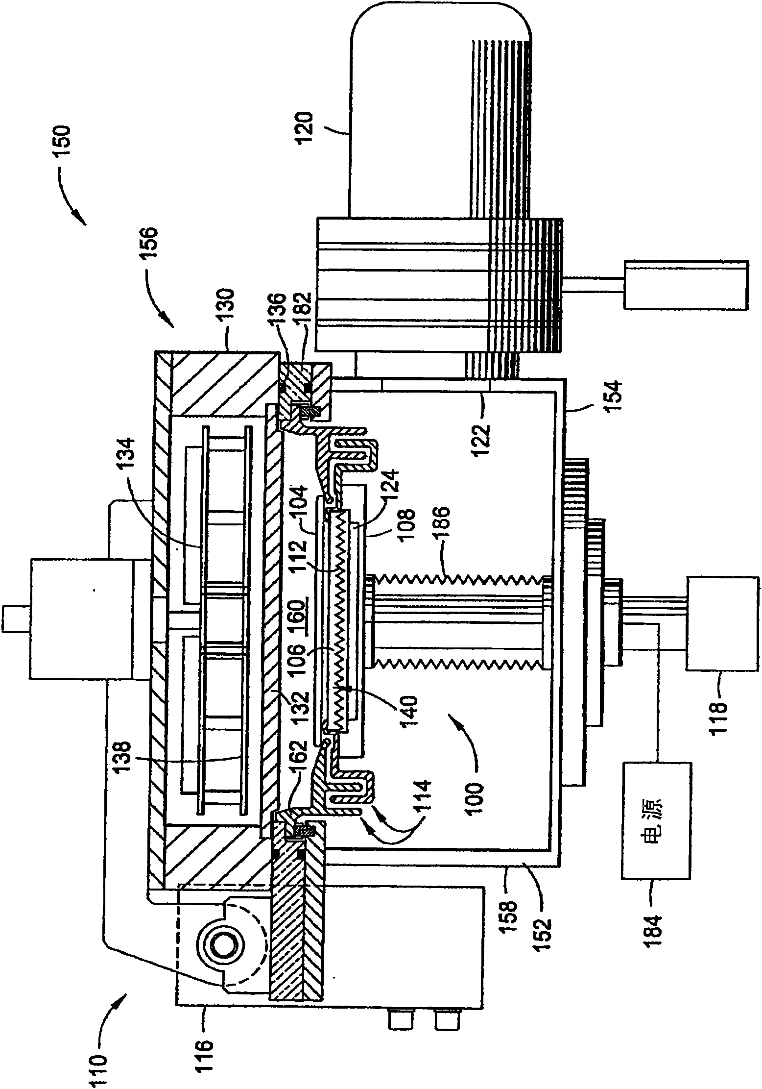
[0020] figure 1 An exemplary semiconductor processing chamber 150 having an embodiment of the processing kit 114 is depicted. The processing suite 114 includes an intersecting deposition ring 102 and a grounded shield 162 . An example of a processing chamber that may benefit from one of the present inventions is the IMPVECTRA available from Applied Materials, Inc., Santa Clara, California. TM PVD treatment chamber. However, it should be understood that other process chambers from other manufacturers may also benefit from the present invention.

[0021] Exemplary processing chamber 150 includes a processing chamber body 152 having a bottom 154 , a lid assembly 156 and a number ...


PUM

PropertyMeasurementUnit
heightaaaaaaaaaa

Abstract

A process kit for use in a physical vapor deposition (PVD) chamber, along with a PVD chamber having a non-contact process kit are provided. In one embodiment, a process kit includes a generally cylindrical shield that has a substantially flat cylindrical body, at least one elongated cylindrical ring extending downward from the body, and a mounting portion extending upwards from an upper surface of the body. In another embodiment, a process kit includes a generally cylindrical deposition ring. The deposition ring includes a substantially flat cylindrical body, at least one downwardly extending u-channel coupled to an outer portion of the body, an inner wall extending upward from an upper surface of an inner region of the body, and a substrate support ledge extending radially inward from the inner wall.

Description

technical field [0001] Embodiments of the invention generally relate to process kits for semiconductor processing chambers and semiconductor processing chambers having processing kits. More particularly, the present invention relates to a process kit including a ring and a shield suitable for use in a physical vapor deposition process chamber. Background technique [0002] Physical vapor deposition (PVD) or sputtering is one of the commonly used processes for manufacturing electronic devices. Physical vapor deposition is a plasma process performed in a vacuum process chamber in which a negatively biased target is exposed to Inert gas voltage. After the ions of the inert gas bombard the target, the atoms of the target material will be ejected. The atoms ejected from the shot accumulate on the substrate on the substrate support seat in the processing chamber to form a deposited film. [0003] A processing kit may be placed in the processing chamber to define a processing r...

Claims


Application Information

Patent Timeline
Patent Type & Authority Applications(China)
IPC IPC(8): F16J15/40
CPCC23C14/564H01L21/68735C23C14/50
Inventor 卡尔·布朗普尼特·班杰
Owner APPLIED MATERIALS INC
Why Eureka
Try Eureka