Optical film production method

A production method and technology for optical films, which are applied in optics, optical components, filters, etc., to achieve the effect of improving process complexity, reducing requirements and costs

Inactive Publication Date: 2011-03-30
BRIVU TECH DANYANG
View PDF5 Cites 0 Cited by
  • Summary
  • Abstract
  • Description
  • Claims
  • Application Information

AI Technical Summary

Problems solved by technology

The materials and processes required to coat the surface of the chip with photoluminescent material greatly increase the cost of LEDs and bring many negative effects
Since the luminescent material is directly coated on the surface of the chip, it increases the difficulty of heat dissipation of the chip, thereby reducing the light conversion efficiency, causing changes in color temperature and chromaticity, and accelerating the aging of the material; inconsistency in color

Method used


Image

  • Optical film production method
  • Optical film production method
  • Optical film production method

Examples


Embodiment Construction

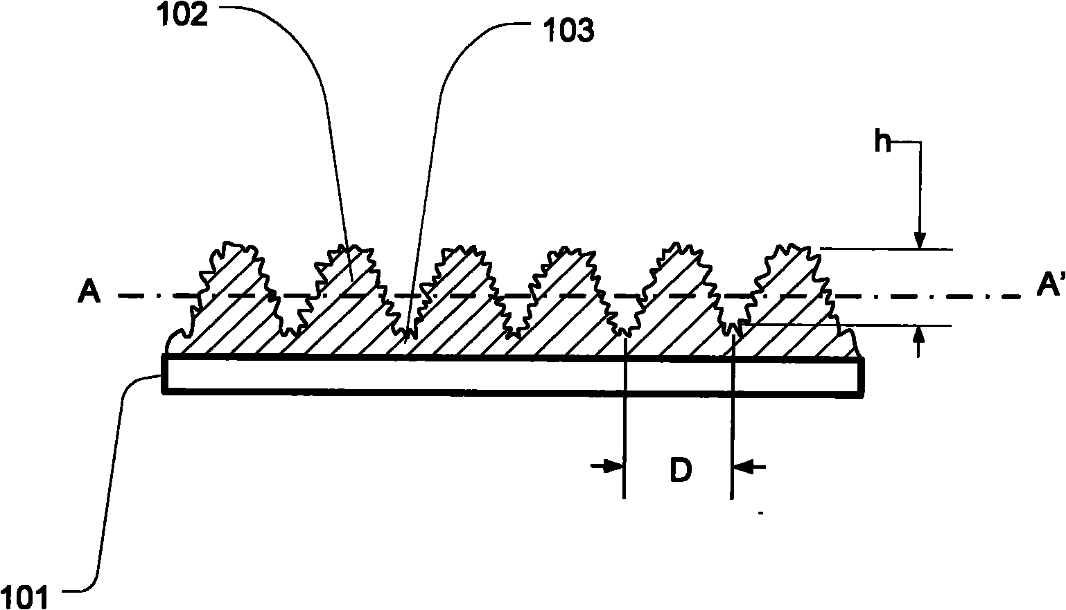
[0030] Depend on figure 1 As known, the optical film 100 includes a base film 101 and a raised microstructure 102 on the surface, and the base film 101 and the raised microstructure 102 are connected by a resin material 103 . The base film 101 is optically transparent, and the material of the base film can be polyester, polyethylene, polycarbonate, such as A-4100 or A-4300 PET film produced by Japan Toyobo. However, the base film material is not particularly limited. Any material with optically transparent properties can be used as the base film material. The raised microstructure 102 may be made of resin material or other materials. When the raised microstructure 102 is made of a resin material, the resin material forming the raised microstructure 102 and the resin material 103 between the microstructures can be the same material or different materials, such as acrylic resin, polyester resin , polyurethane, polyvinyl chloride, or silicone. The raised microstructure 102 c...


PUM

PropertyMeasurementUnit
thicknessaaaaaaaaaa
heightaaaaaaaaaa
sizeaaaaaaaaaa

Abstract

The invention relates to a production method of an optical film, which comprises the steps of: (1) preparing material mixtures; (2) coating the material mixtures; (3) selectively polymerizing the material mixtures; (4) washing; and (5) curing. The invention better decreases the number of optical elements needed by a liquid crystal display and an illumination light source, reduces the technological cost, overcomes the detects of complex process and higher cost of a brightness enhancement film used for the traditional display and can reduce the requirement for an LED and the cost of the LED when combined with the LED for use.

Description

technical field [0001] The present invention relates to liquid crystal display and LED energy-saving lighting materials, in particular to a three-dimensional microstructure brightening optical film used in mobile phones, portable computers, desktop computers, LCD TVs and other liquid crystal display backlight modules and LED energy-saving lighting components and its production method. technical background [0002] Among various light sources used in liquid crystal display and lighting, brightness and luminous efficiency are very important parameters. In order to achieve such an effect, numerous optical components and high-cost processes are usually required. For example, in the backlight of a liquid crystal display, the light emitted from the cold cathode lamp (CCFL) and the light emitting diode (LED) needs to pass through the light guide plate, and the diffusion film reaches the liquid crystal panel. In order to increase the brightness of the display, it is usually neces...

Claims


Application Information

Patent Timeline
Patent Type & Authority Patents(China)
IPC IPC(8): G02B5/20F21V9/10G02B1/00F21V9/40
CPCY02B20/181Y02B20/00
Inventor 路志坚杨星杨云胜束国法
Owner BRIVU TECH DANYANG
Why Eureka
Try Eureka