In situ evaluation system and method of reliability of thin-film materials on flexible electronic substrate

A thin film material, in-situ test technology, applied in the direction of testing the strength of the material by applying a stable bending force, can solve the problems of large cracking and strain errors of the thin film material, and the inapplicability of the resistance method of the non-conductive thin film material, etc., so as to improve the test accuracy, Easy to prepare and wide range of applications

Inactive Publication Date: 2011-09-21
INST OF METAL RESEARCH - CHINESE ACAD OF SCI
View PDF0 Cites 0 Cited by
  • Summary
  • Abstract
  • Description
  • Claims
  • Application Information

AI Technical Summary

Problems solved by technology

[0004] The purpose of the present invention is to provide an accurate, simple and fast in-situ evaluation system and method for the reliability of single-layer or multi-layer thin film materials on flexible electronic substrates with a thickness of micron to nanometer. The in-situ test system and test method characterize the thin film The critical strain at the initiation of material damage solves the problems in the prior art that the cracking strain error of thin film materials is large, and the resistance method cannot be applied to non-conductive thin film materials.

Method used


Image

  • In situ evaluation system and method of reliability of thin-film materials on flexible electronic substrate
  • In situ evaluation system and method of reliability of thin-film materials on flexible electronic substrate
  • In situ evaluation system and method of reliability of thin-film materials on flexible electronic substrate

Examples


Embodiment 1

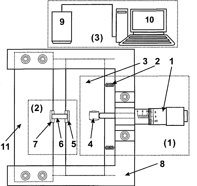
[0056] The principle diagram of the in-situ evaluation system of the present invention is as figure 1 shown.

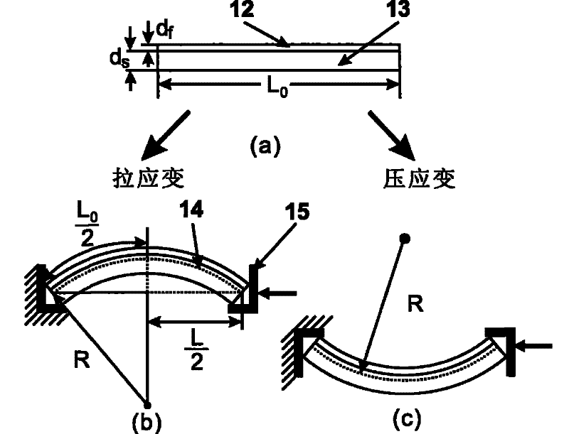
[0057] Cu-Ni multilayer films with a total thickness of 1 μm and a single layer thickness of 50 nm were prepared on a polyimide substrate with a thickness of 125 μm by magnetron sputtering. Cut the sample into a rectangle with a size of 12 mm x 2 mm. First, according to the original length of the sample, adjust the distance between the movable end of the simply supported beam and the fixed end of the simply supported beam of the test system to an appropriate distance that matches the size of the sample. according to figure 2 In the placement state shown in (b), the sample is placed above the simple support point 15, and the translational slider 3 is driven by the screw micrometer 1 and the balance spring 2 to move slightly horizontally, and the sample 6 is positively bent, so that the Cu-Ni multilayer film on polyimide substrate exerts constant tensile strain. Re...

Embodiment 2

[0059] Cu-Ta multilayer films with a total thickness of 1 μm and a single layer thickness of 50 nm were prepared on a polyimide substrate with a thickness of 125 μm by magnetron sputtering. Cut the sample into a rectangle with a size of 12 mm x 2 mm. First, adjust the distance between the movable end of the simply supported beam and the fixed end of the simply supported beam of the test system to a suitable distance according to the original length of the sample, as figure 2 As shown in (c), in this placement state, the sample is placed on a simple support point, and the translational slider 3 is driven to move horizontally by the screw micrometer 1 and the balance spring 2, and the sample 6 is reversed, so that the polyimide The Cu-Ta multilayer film on the substrate exerts a constant compressive strain. Record the distance L of the simple support point, and simultaneously collect images of the surface topography of the sample through a high-power optical microscope and a C...


PUM

PropertyMeasurementUnit
thicknessaaaaaaaaaa

Abstract

The invention relates to establishment for a test device and a test method for the bending fracture performance of thin-film materials, in particular to an in situ evaluation system and a method of the mechanical reliability of a layer or a plurality of layers of thin-film materials with the micron to nanometer thickness on a flexible electronic substrate. The system comprises a high-precision micrometer caliper, a balance spring, a translational slide block, a freely supported beam fixed end, a freely supported beam movable end, and the like, wherein a composite beam comprising the micrometer caliper and a flexible substrate exerts precise and controllable step displacement to implement freely supported beam bending experiments; real-time exerted strain corresponding to a freely supported beam span is computed according to parameters and geometrical relationship of the freely supported beam span, sample sizes, and the like; and the bending fracture performance and critical cracking strain of the kind of thin film are tested and evaluated by combining in situ microscopic observation and subsequent scanning electron microscope characterization. The invention does not need to consider the electroconductibility of the thin-film materials, and is still adaptable for non-conductive thin-film materials. The experiment operation is simple and fast, in situ real-time positioning observation and analysis can be carried out on samples.

Description

technical field [0001] The present invention relates to the establishment of testing devices and testing methods for the bending and fracture performance of various thin film materials, specifically an in-situ testing system and method for the reliability of thin film materials on flexible electronic substrates, and is especially suitable for testing the reliability of thin film materials prepared on flexible electronic substrates. Test the fracture performance of single-layer or multi-layer film materials with micron, submicron and nanometer thickness. Background technique [0002] Flexible electronic devices have broad application prospects, such as rollable liquid crystal displays, flexible solar panels, and electronic paper. Single-layer and multi-layer film materials with micron, submicron and nanometer thickness attached to flexible base media are widely used in circuit interconnection wiring and barrier layers in the above-mentioned devices. The above-mentioned devic...

Claims


Application Information

Patent Timeline
Patent Type & Authority Patents(China)
IPC IPC(8): G01N3/20
Inventor 张广平朱晓飞张滨
Owner INST OF METAL RESEARCH - CHINESE ACAD OF SCI
Why Eureka
Try Eureka