A Method for Analyzing Displacement Damage Effects of CMOS Devices

A technology of displacement damage and devices, applied in instruments, special data processing applications, calculations, etc.

Inactive Publication Date: 2012-02-01
SEMICONDUCTOR MANUFACTURING INTERNATIONAL (BEIJING) CORP +1
View PDF0 Cites 0 Cited by
  • Summary
  • Abstract
  • Description
  • Claims
  • Application Information

AI Technical Summary

Problems solved by technology

[0004] Therefore, with the improvement of circuit integration, the method used to predict the single event effect of devices and integrated circuits is no longer accurate. Cannot meet the application of current irradiation technology

Method used


Image

  • A Method for Analyzing Displacement Damage Effects of CMOS Devices
  • A Method for Analyzing Displacement Damage Effects of CMOS Devices
  • A Method for Analyzing Displacement Damage Effects of CMOS Devices

Examples


Embodiment Construction

[0030] The preferred embodiment of the present invention is described in more detail below with reference to the accompanying drawings of the present invention.

[0031] The following is a detailed description of six sub-analysis modules of the present invention:

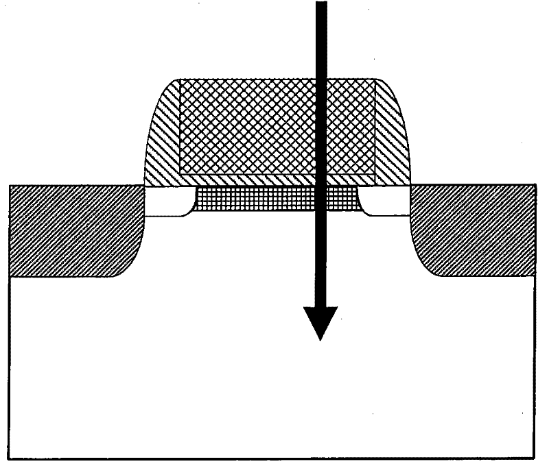
[0032]A drain and source displacement damage analysis module: displacement damage leads to effective gate-source voltage V gseff and the drain-source voltage V dseff reduce. With the shortening of the channel length of the MOS transistor, the intrinsic resistance of the channel decreases, but the parasitic resistance of the source and drain regions will not shrink in proportion, which makes the influence of the parasitic resistance larger. Since the heavy particles hit near the source and drain of the device, the displacement damage caused by the irradiation causes the parasitic resistance of the source and drain to increase, and the parasitic source and drain resistance makes the effective V gseff and V dseff d...


PUM


Abstract

The invention provides a model for analyzing radiation displacement damage of CMOS devices, belonging to the technical field of radiation displacement damage of CMOS devices. The model consists of six sub-analysis modules, including: a drain and source displacement damage analysis module, a channel region displacement damage analysis module, a defect group analysis module, a composite enhanced migration analysis module, and a transient enhanced diffusion analysis module and an isolation zone displacement damage analysis module, using the Monte Carlo method to randomly generate incident particles according to a Gaussian distribution, the model obtains one or more values ​​in the above six sub-analysis modules according to the position where the incident particles enter the device, and obtains Displacement damage effects of CMOS devices under irradiation conditions. The invention can accurately estimate the displacement damage effect of the device and the integrated circuit in the radiation environment.

Description

technical field [0001] The invention relates to integrated circuit anti-irradiation technology, in particular to a model for analyzing the effect of displacement damage on the electrical characteristics of CMOS devices. Background technique [0002] CMOS integrated circuits have followed Moore's Law for decades. The level of integration continues to increase through shrinking device dimensions. As device feature sizes shrink, device performance continues to evolve. However, the reduction in device feature size also brings various downsizing effects and reliability issues. Small size effects mainly include severe degradation of subthreshold characteristics, DIBL (drain-induced barrier reduction), and threshold voltage is very seriously related to channel length; reliability problems mainly include hot carrier effects, oxide layer over time Breakdown (TDDB) and degeneration of PN junction, etc. In order to make deep submicron devices work properly, various improvements ha...

Claims


Application Information

Patent Timeline
Patent Type & Authority Patents(China)
IPC IPC(8): G06F17/50
Inventor 薛守斌王思浩安霞黄如张兴
Owner SEMICONDUCTOR MANUFACTURING INTERNATIONAL (BEIJING) CORP
Why Eureka
Try Eureka